In this article, you will learn what a snubber circuit is and why we need to use it with power electronics circuits across semiconductor switches. We will also explore the different types commonly used in power electronics circuits.
What is a Snubber Circuit?
A snubber circuit is essentially an RC circuit used to minimize the back EMF voltage or dv/dt within a semiconductor diode’s limit. It is connected across semiconductor devices and plays a vital role in power electronics circuits. The circuit provides protection to the semiconductor devices used in power electronics circuits, ensuring they are shielded from reverse voltage.
Types
There are three types of snubber circuits commonly used in power electronics circuits. Let’s explore each of them:
Forward Polarized Snubber Circuit
This type of circuit is more suitable when a diode is connected anti-parallel to a transistor or thyristor. The circuit diagram for a forward-polarized snubber is shown below:
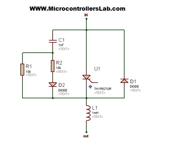
The resistor R1 is used to limit the dv/dt voltage across the semiconductor device, while resistor R2 controls the discharging current of capacitor C1 during the turn-on time of the semiconductor device.
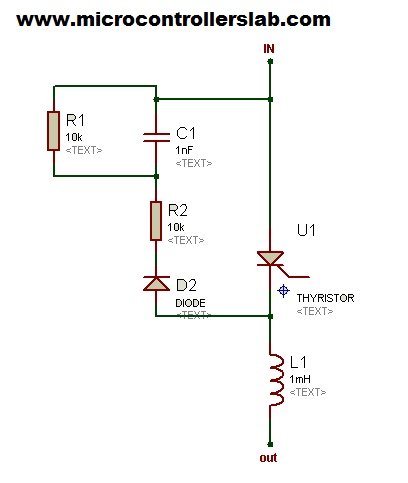
Reverse Polarized Snubber Circuit
The circuit diagram for a reverse polarized snubber is shown below. In this configuration, resistor R1 limits the reverse voltage dv/dt, and R2 discharges the capacitor. The advantage of a reverse polarized snubber circuit is that the capacitor does not discharge through the semiconductor device, thereby reducing losses.
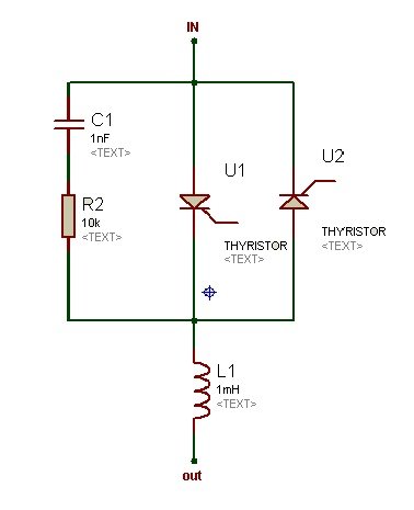
Unpolarized Snubber Circuit
Unpolarized snubber circuits are used when two semiconductor devices are connected anti-parallel to each other, as shown in the figure below. In this scenario, the snubber circuit needs to work in both directions, which is why an unpolarized snubber is used. The circuit diagram for an unpolarized is shown below:
To design this circuit, you need to consider the following factors:
- Reverse recovery time of the semiconductor device
- Current rating of the semiconductor device
- Total circuit inductance
- Input voltage to the circuit
- Optimum value of current factor (can be found in the datasheet of the semiconductor device)
- Optimum damping factor
If you have the above information, you can calculate the values of the capacitor and resistors using the following formulas:
C = L * (Ir / dVs)²
R = 2δ * √(LC)
Applications
These circuits are used in electronics and electrical systems to control or suppress voltage spikes, transient overvoltages, and ringing in various types of circuits and components. These voltage spikes and transients can occur due to inductive or capacitive loads, switching actions, or other disturbances in the circuit. These circuits help improve the overall reliability, performance, and lifespan of components and systems by mitigating these unwanted effects. Here are some common applications of snubber circuits:
- Power Electronics:
In switching power supplies, snubber circuits can be employed across switches (such as power transistors or diodes) to dampen voltage spikes generated during switching transitions. This reduces stress on the switches and minimizes electromagnetic interference (EMI).
In AC-DC converters and DC-DC converters, snubber circuits can suppress voltage spikes caused by transformer leakage inductance or parasitic capacitance, enhancing efficiency and reducing EMI.
- Motor Control:
Snubber circuits can be used in motor drive applications to suppress voltage spikes and ringing that occur when switching the direction of current flow or during rapid changes in current direction.
- Relay and Switching Circuits:
They can be applied across relays and switches to reduce arcing and contact wear during opening or closing operations. This helps extend the lifespan of these components.
- Inductive Loads:
Snubber circuits are commonly used with inductive loads such as solenoids, coils, and transformers to prevent voltage spikes and ringing that can occur when the current through the inductor is interrupted.
- Solid-State Devices:
In applications involving solid-state devices like thyristors and triacs, snubber circuits can be used to prevent false triggering or unintended turn-on due to voltage spikes or noise.
- LED Lighting:
Snubbers can be used in LED lighting circuits to suppress voltage spikes that can occur when the LED driver switches on or off. This helps prevent damage to the LEDs and ensures consistent performance.
- Electronic Ballasts:
In fluorescent lamp ballast circuits, snubber circuits can be applied to mitigate voltage spikes and ringing caused by inductive loads and switching.
- Motor Protection:
These circuits can be used to protect motors from voltage spikes generated during the opening of mechanical contacts, preventing damage to the motor windings.
- Power Factor Correction (PFC):
Snubbers can be used in power factor correction circuits to suppress voltage spikes that can occur when reactive components are switched in and out of the circuit.
Conclusion
In conclusion, a snubber circuit is a crucial component in power electronics circuits that helps protect semiconductor devices from reverse voltage and minimize back EMF voltage. There are three common types of circuits: forward polarized, reverse polarized, and unpolarized. Each type has its own advantages and is used in specific configurations. When designing a snubber circuit, several factors must be taken into consideration, such as the semiconductor device’s reverse recovery time, current rating, circuit inductance, and input voltage. By calculating the appropriate values for capacitors and resistors, one can ensure the optimal performance of the circuit. Understanding and implementing snubber circuits can greatly enhance the reliability and efficiency of power electronics systems.
Related content:
hi…. i am doing my third year in ece….i am doing my mini project. my topic is GSM BASED VEHICLE THEFT INTIMATION USING PIC MICROCONTROLLER(16F877A). i have pic board with max232 and a RESET button. with the help of this rest button the PIC microcontroller should identify the UNAUTHORISEDD UESR. I am not clear with the program to be done in PIC microcontroller with the reset button…can anyone pls help to solve this problem
I also provide project services if you need project services contact me at microcontrollerslabhub@gmail.com
salut à touts,
je fais ma projet PFE et Je suis en train de faire mon simulation et la réalisation de circuit (clac). mon sujet est étude et modélisation d’un circuit d’aide à la commutation à base éléments non linéaires . l’élément non linéaire qui en utilise ici c’est cendansateur céramique BaTiO3 elle à une caractiréstique de minimisé des perts dues à la commutation pour limiter dv/dt. dans ma projet en utilise un bras hacheur … j’ai besion état de l’art de circuit simulation avec PSIM et quelque documentation
merci
salut
je fais mon projet PFEet Je suis en train de faire simulisaton et la réalisation de projet. mon sujet est : étude et modélisation d’un circuit d’aide à la commutation à base élement non léniaire. l’élément non linéaire ici cendansateur céramique BaTiO3 en utilise cette circuit “snubber” pour limiter les perts (dv/dt) dans mon projet en utilise un bras hacheur ….j’ai besion état l’art de mon simulation sur POWERSIM et les documentation cencernant le sujet
merci