In this article, you will learn everything you need to know about printed circuit boards (PCBs). A printed circuit board is extremely important for electronics engineers in order to create electronic circuits. Many electronics and electrical engineers often overlook the importance of this technique, and some engineers may not even know what a printed circuit board is exactly. If you are unfamiliar with PCBs, this article will provide you with useful knowledge regarding their design. Additionally, I have included video tutorials at the end of this article. These tutorials demonstrate how to design a printed circuit board using Proteus software.

In this article you will learn:
- What is a printed circuit board?
- What are the layers of a printed circuit board? What is the copper side of a printed circuit board?
- What are traces in a printed circuit board and how do you select their width?
- Are there any video tutorials available for PCB designing?
What is a PCB?
As the name suggests, a Printed Circuit Board (PCB) is a board on which a circuit is printed using a specific procedure. It is a type of board that connects various components together through copper traces on the board. It is made of copper. A proper procedure is used to print the circuit on the board, and I will discuss this procedure in video tutorials with practical examples. Before the invention of the Printed Circuit Board, circuits were made using connecting wires, which was a very hectic and time-consuming process. With the invention of this technique, you can even make a PCB at home with ease. These boards are widely used in electronic devices such as computer motherboards, and mobile boards, and nearly every single electronic device contains a printed circuit board inside. The diagram above shows a power supply printed circuit board.

What are layers in PCB design?
Layers are the most important key points in its design. It can be made with up to 12 layers, but the maximum circuits available in the market are single layer. Now, the question comes into someone’s mind: what is a layer? To better understand what a layer is, have a look at the pictures shown below:
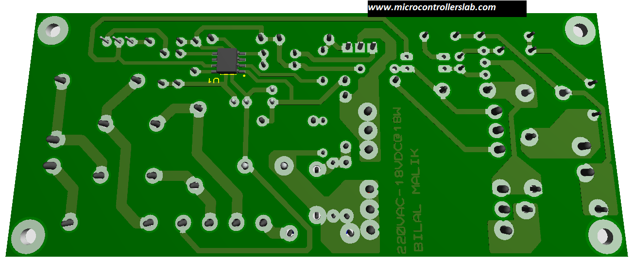
As shown in the above picture, there are traces of copper which are used to connect components to each other, and it is basically a layer of the board. The above diagram is a single-layer board because it has copper layers only on one side of the board, and the other side of the above board is for the placement or assembly of components. I will discuss in a video training how to make such boards. The diagram below shows the top view of a board where we place components, and it is called the top silk of the printed circuit board.

What are Traces in PCBs and How to Select their Width?
Traces are made of copper which are used to connect points with each other. In other words, they are the lines through which current flows from one point to another point. There are usually two types of traces.
- Signal Traces
- Power Traces
Signal traces’ width is small, while power traces’ width is larger. The width of Power traces is determined by the amount of current flowing through them. Signal traces, on the other hand, are typically narrower as the current flowing through them tends to be in milliamperes. Now, the question is how to determine the appropriate trace width based on the current magnitude. The answer to this question is provided in video tutorials that are mentioned at the end of this article. The diagram below illustrates the power and signal traces on the board. The yellow arrow indicates signal traces, while the black arrow indicates power traces.

Video Tutorial on PCB Designing Using Proteus ARES
In these video tutorials, you will learn how to use Proteus ARES software for PCB designing. There are many software options available for PCB designing, such as Orcad, Eagle, and Express PCB. However, if you are a beginner in designing, I recommend using Proteus ARES as it is easy to use. In the coming weeks, I will also post articles on Eagle and Orcad for their respective design processes. I assure you that after watching the following video tutorials, you will be able to create your own board. To become a professional in circuit designing, it is essential to practice different examples. Good luck!
Tutorial number: 1 Basic overview of PCB designing and schematic diagrams
Tutorial Number 2: What is a PCB Package? And How to Use It?
In this tutorial, we will discuss the concept of a PCB package and its usage.
Tutorial Number: 3 – Complete PCB Designing with Example
Tutorial Number 4: Complete PCB Designing with Example Part 2
I will also add a video tutorial about how to make a PCB package in Proteus if it is not available. If you have any issues while doing PCB designing, let me know in the comments. I will try to answer your questions as soon as possible. This is all the effort from my side to help others who want to learn circuit designing. What can you do right now to help others? Just share this post with your friends and juniors by clicking on the social sharing buttons shown below. That’s what you can do right now. Thanks 🙂
good article very helpful.
Helpful article and source of info for engineers.
You did not told in any tutorial that how to make pcb package if it is not available in proteus???
THANKS
Great work and helpful, please can the English version be avaliable
Hello, Bilal Malik, my problem is how to transfer the designed work onto the pc board. Method for how do that is what I am requiring for. Please let me have it. Thank you.
hi everybody.can u send 4 me hybrid inverter pcb complete.plz send 4 me
excellent work………….bro
Positive people see an opportunity in every worry, while negative people see some kind of worry in every opportunity.