INTRODUCTION TO PIC18F4550 MICROCONTROLLER: The PIC18F is one of the families of pic microcontrollers and PIC18F4550 is its member. PIC18F4550 is one many of the advanced microcontrollers from the microchip era. This microcontroller is very famous in between hobbyist and beginners due it functionalities and functions along with ADC and USB integration. There are different packages like DIP, QPF, and QPN of PIC18F4550 which are currently available.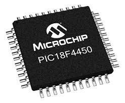
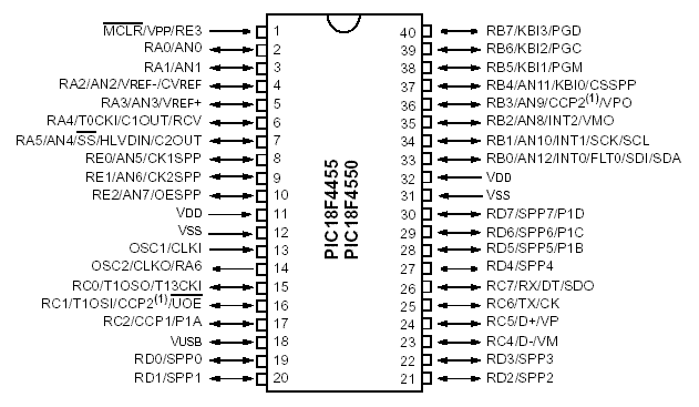
Pin out of PIC18F4550 microcontroller
Pin diagram of this microcontroller is given. It has 40 pins.
FEATURES OF PIC18F4550
- NANO WATT GENERATION: PIC18F4550 is an 8-bit microcontroller. PIC18F4550 has been applied with NANO WATT technology, therefore, it requires very low strength for its operation. Some of the important features of this microcontroller are:
- ALTERNATE RUN MODES: When cocking the controller by timer1 source or any internal oscillator block, the power can be reduced during execution of code up to 90%.
- MULTIPLE IDLE MODES: It has the advantage of working even when its CPU disabled but peripherals being active. The power can be reduced up to 4% in these states.
- ON-THE-FLY MODE SWITCHING: It is the power managed modes which referred by user code during operation. It allows the user to implement different ideas of power-consumption into their design of application software.
- LOW CONSUMPTION IN KEY MODULES: The Timer1 and watchdog both have low power requirements.
- UNIVERSAL SERIAL BUS: The PIC18F4550 implements complete features universal serial bus communications module supporting low-speed and full-speed communication with any type of data transfer. It also has its own on-chip transceiver and 3.3V regulator supporting the use of external transceiver and voltage regulators.
- MULTIPLE OSCILLATOR OPTIONS AND FEATURES: The devices in PIC18F4550 supports twelve different options of the oscillator which makes the user have a range of choices for developing any application hardware. These options are:
- Four crystal modes the use of crystals or ceramic resonators.
- 4 external clock modes, imparting the choice of using two pins (oscillator enter and a divide with the aid of-4 clock output) or one pin (oscillator input, with the second one pin, reassigned as fashionable I/O).
- an inner oscillator block which affords an 8 MHz clock (±2% accuracy) and an INTRC source (about 31 kHz, stable over temperature and Voo), in addition to a range of 6 person-selectable clock frequencies, between a hundred twenty-five kHz to four MHz, for a total of eight clock frequencies. This feature releases an oscillator pin for use as a further well-known object I/O.
- A phase lock loop (PLL) frequency multiplier, available to each the high-velocity crystal and outside oscillator modes, which lets in an extensive range of clock speeds from 4 MHz to 48 MHz
- Asynchronous dual clock operation, allowing the USB module to run from a high-frequency oscillator whilst the relaxation of the microcontroller is clocked from an inner low-power oscillator.
Besides its availability as a clock source, the inner oscillator block presents a strong reference source that offers the own family extra functions for strong operation:
- FAIL-SAFE CLOCK DISPLAY: This option continuously monitors the principle clock supply against a reference sign furnished via the internal oscillator. If a clock failure occurs, the controller is switched to the internal oscillator block, taking into account persevered low-pace operation or a safe software shutdown.
- TWO-VELOCITY BEGIN-UP: This option permits the inner oscillator to serve as the clock supply from energy on reset, or wake-up from sleep mode, till the primary clock supply is available.
OTHER SOME SPECIAL FEATURES
- MEMORY ENDURANCE: The improved flash cells for each software memory and statistics EEPROM are rated to final for many heaps of erase/write cycles – up to one lac for application memory and a million for EEPROM. Information maintenance without refresh is conservatively expected to be more than forty years.
- SELF-PROGRAMMABILITY: These gadgets can write to their own application reminiscence spaces underneath inner software manipulate. By means of the use of a boot loader ordinary, located in the blanketed boot block on the pinnacle of application reminiscence, it will become viable to create a utility which could replace itself inside the field.
- EXTENDED INSTRUCTION SET: The PIC18F4550 own family introduces a non-obligatory extension to the PIC18 preparation set, which adds eight new commands and an indexed literal offset addressing mode. This extension enabled as a device configuration choice, has been mainly designed to optimize re-entrant software code at the beginning advanced in excessive-degree languages together with C.
- ENHANCED CCP MODULE: In PWM mode, this module provides 1, 2 or 4 modulated outputs for controlling half-bridge and complete bridge drivers. Different functions consist of vehicle shutdown for disabling PWM outputs on interrupt or different choose situations, and automobile-restart to reactivate outputs once the situation has cleared.
- ENHANCED ADDRESSABLE USART: This serial verbal exchange module is able to a well-known RS-232 operation and affords aid for the LIN bus protocol. The TX/CK and RX/DT alerts can be inverted, eliminating the need for inverting buffers. Other upgrades encompass computerized baud rate detection and a 16-bit baud price generator for progressed resolution. When the microcontroller is the usage of the inner oscillator block, the EUSART affords a stable operation for packages that speak to the outside global without the use of an outside crystal (or its accompanying electricity requirement).
- 10-BIT A/D CONVERTER: This module contains programmable acquisition time, allowing for a channel to be decided on and a conversion to be initiated, without waiting for a sampling period and for this reason, reducing code overhead.
Check this complete tutorial on tutorial on how to use PIC18F4450 microcontroller ADC with programming in MPLAB XC8 Compiler:
- DEDICATED ICD/ICSP PORT: Those devices introduce the usage of debugger and programming pins that aren’t multiplexed with different microcontroller functions. Provided as an option in pick programs, this option permits users to develop I/O extensive packages while maintaining the capability to an application and debug inside the circuit. it is stronger flash application and the 1kb dual access ram for USB are used for buffering.
- Input / Output Ports: It has 5 input output ports. Each post consists of eight pins. Each pin has more than one functions. The function of each pin can be selected through special function registers. For example, TRISD register is used to select the direction of PORTD pin either as an input or output. Similarly, PORTC can be used as an input or output but it also has functions of PWM and serial communication. The function of each pin can be selected through special function registers.
- Timers: PIC18F4550 microcontroller has three timers Timer0, timer1, and timer2. Each timer can be used as a timer or counter depending on the application. Timers can bed used be used to generate delays.
- Interrupts: PIC18F4550 microcontroller has multiple interrupts with a priority feature. Priority can be assigned to each interrupt. High priority interrupts can stop low stop interrupts from execution.
The PIC18F4550 consists of up to 13 channels for analog to digital converter. The converter accuracy quantities to ten-bit to convert analog to digital sign particularly. It is well matched to work with unique inner and outside clock resources. It comes with 4 built-in timers or an external oscillator may be interfaced for clocking. The frequency range is from 31 kHz to 48 MHz respectively. The microcontroller PIC18F4550 comes with ADC comparators and different such peripherals.