dspic33fj12GP202 microcontroller based sinusoidal pulse width modulation generation. Hi Everyone, I hope you are fine and doing well. In this article you will learn how to generate sinusoidal pulse width modulation using dspic33fj12GP202 microcontroller. I have found many people searching on internet regarding how to generate SPWM using DSpic microcontroller. So I will explain here how to generate SPWM using built in PWM module of dspic33fj12GP202 microcontroller. SPWM generation is very important in power electronics projects. I have already posted many project related to power electronics inverters. you may also like to check them.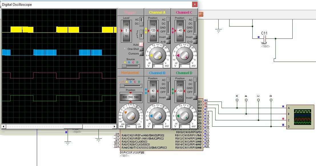
- SPWM generation using pic16f877a microcontroller
- single phase pure sine wave inverter using pic microcontroller
- Modified sine wave inverter using pic16f877a
- solar inverter
- three phase sine wave inverter using Arduino
- Single phase sine wave inverter using Arduino
So in this project, we will create sinusoidal pulse width modulation using dspic33fj12GP202. Mostly pure sine wave inverters available in market use dspic microcontrollers due to its high performance and high speed calculation power. I have used dspic33fj12GP202 in this tutorial. But same logic can be applied to any DsPIC series of microcontrollers. Let’s start with the introduction of dspic33fj12GP202 features which are used for SPWM generation.
Output compare module of dspic33fj12GP202 in PWM mode for sinusoidal pulse width modulation generation
Output compare module of dspic33fj12GP202 microcontroller is used in PWM mode to generate SPWM. This module use two sixteen bit timers that is Timer 2 and Timer 3. OCM compares the set value of timer register with OCM registers OCxR and OCxRS. When both values becomes equal to each other, state of output pin changes. It happens only once in one period of PWM. dspic33fj12GP202 contains 2 output compare modules. So we can can generate only two PWM with the help of this DsPIC microcontroller. Output compare control registers for dspic33fj12GP202 microcontroller is given. 

Above register details shows how to use dspic33fj12GP202 output compare as a PWM. It can use either TIMER2 or TIMER3 as a time setting which can be configured through OCTSEL bit of OCxCON register as shown above. So I have used output compare module as a PWM to generate sinusoidal pulse width modulation. PRy register is used to set period or frequency of PWM.
Generation of sinusoidal pulse width modulation generation using dspic33fj12GP202 microcontroller
To generate SPWM, we want to generate square wave with different duty cycle. I have done it through look up table. I have used different square waves with different duty cycle to get pure sine wave from SPWM signals. The more is the number of square waves, more clean sine wave we will get at the output of inverter. I have generated a sine table with 512 values for complete complete sine wave which is given below:
const int sin_table[512] =const int sin_table[512] ={0, 5, 10, 15, 20, 25, 29, 34, 39, 44, 49, 54, 59, 64, 68, 73,78, 83, 88, 92, 97, 102, 107, 111, 116, 121, 125, 130, 135, 139,144, 149, 153, 158, 162, 167, 171, 175, 180, 184, 189, 193, 197,201, 206, 210, 214, 218, 222, 226, 230, 234, 238, 242, 246, 250,254, 258, 261, 265, 269, 272, 276, 279, 283, 286, 290, 293, 296,300, 303, 306, 309, 312, 315, 318, 321, 324, 327, 330, 333, 335,338, 341, 343, 346, 348, 350, 353, 355, 357, 359, 362, 364, 366,368, 370, 371, 373, 375, 377, 378, 380, 381, 383, 384, 386, 387,388, 389, 390, 391, 392, 393, 394, 395, 396, 396, 397, 398, 398,399, 399, 399, 400, 400, 400, 400, 400, 400, 400, 400, 400, 399,399, 399, 398, 398, 397, 396, 396, 395, 394, 393, 392, 391, 390,389, 388, 387, 386, 384, 383, 381, 380, 378, 377, 375, 373, 371,370, 368, 366, 364, 362, 359, 357, 355, 353, 350, 348, 346, 343,341, 338, 335, 333, 330, 327, 324, 321, 318, 315, 312, 309, 306,303, 300, 296, 293, 290, 286, 283, 279, 276, 272, 269, 265, 261,258, 254, 250, 246, 242, 238, 234, 230, 226, 222, 218, 214, 210,206, 201, 197, 193, 189, 184, 180, 175, 171, 167, 162, 158, 153,149, 144, 139, 135, 130, 125, 121, 116, 111, 107, 102, 97, 92, 88,83, 78, 73, 68, 64, 59, 54, 49, 44, 39, 34, 29, 25, 20, 15, 10, 5,0, 5, 10, 15, 20, 25, 29, 34, 39, 44, 49, 54, 59, 64, 68, 73,78, 83, 88, 92, 97, 102, 107, 111, 116, 121, 125, 130, 135, 139,144, 149, 153, 158, 162, 167, 171, 175, 180, 184, 189, 193, 197,201, 206, 210, 214, 218, 222, 226, 230, 234, 238, 242, 246, 250,254, 258, 261, 265, 269, 272, 276, 279, 283, 286, 290, 293, 296,300, 303, 306, 309, 312, 315, 318, 321, 324, 327, 330, 333, 335,338, 341, 343, 346, 348, 350, 353, 355, 357, 359, 362, 364, 366,368, 370, 371, 373, 375, 377, 378, 380, 381, 383, 384, 386, 387,388, 389, 390, 391, 392, 393, 394, 395, 396, 396, 397, 398, 398,399, 399, 399, 400, 400, 400, 400, 400, 400, 400, 400, 400, 399,399, 399, 398, 398, 397, 396, 396, 395, 394, 393, 392, 391, 390,389, 388, 387, 386, 384, 383, 381, 380, 378, 377, 375, 373, 371,370, 368, 366, 364, 362, 359, 357, 355, 353, 350, 348, 346, 343,341, 338, 335, 333, 330, 327, 324, 321, 318, 315, 312, 309, 306,303, 300, 296, 293, 290, 286, 283, 279, 276, 272, 269, 265, 261,258, 254, 250, 246, 242, 238, 234, 230, 226, 222, 218, 214, 210,206, 201, 197, 193, 189, 184, 180, 175, 171, 167, 162, 158, 153,149, 144, 139, 135, 130, 125, 121, 116, 111, 107, 102, 97, 92, 88,83, 78, 73, 68, 64, 59, 54, 49, 44, 39, 34, 29, 25, 20, 15, 10, 5};
Each value of lookup table is the value of period register which will change after one complete period. The frequency of PWM is 25kHz. So each pulse will be of 40us with different duty cycles. After 512 square wave, total time will be 20ms which is 50HZ required frequency of our sinusoidal pulse width modulation.
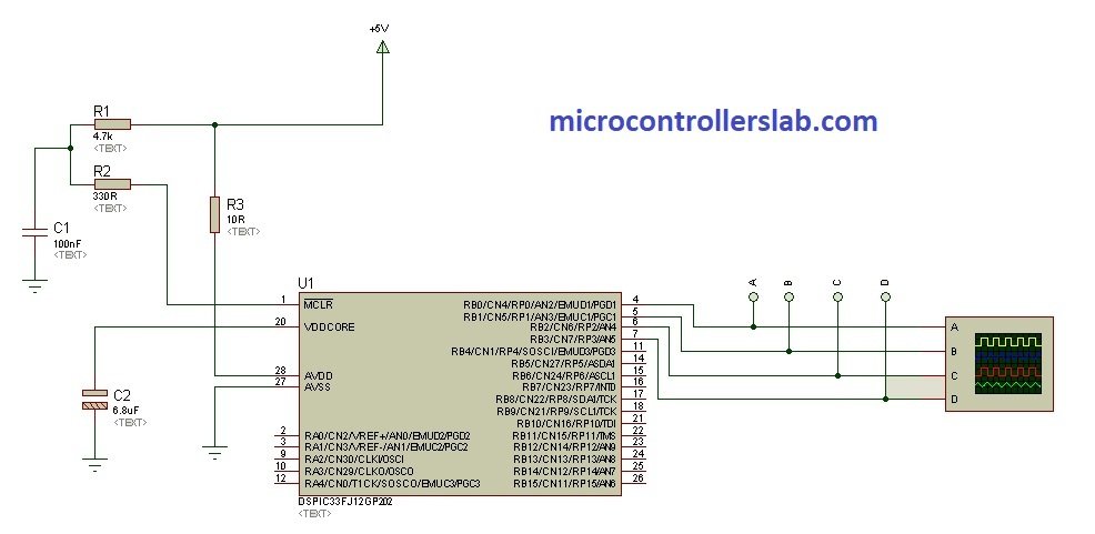
sinusoidal pulse width modulation generation circuit diagram
Proteus simulation of sinusoidal pulse width modulation generation with dspic33fj12GP202
Contact us for source code.
Hello, does the code include grid charging? if so I would like to have it.
Hello I want write software a inverter motors please helpme
Very useful for beginners. If the source code with purpose of each step is explained, it will really help beginners as most of the time how to configure the particular pin for output is not clearly described in datasheet.