The 74HCT04 IC is a hex inverter IC which is composed of six independent inverters with standard push-pull outputs. It is a high-speed inverter whose pins are low power Schottky (LSTTL) compatible. All the inputs are protected from electric discharges through the diodes protection network which provides protection from input voltages in excess of Vcc by enabling the use of current limiting resistors. It can operate within a range of -40°C to +125°C.
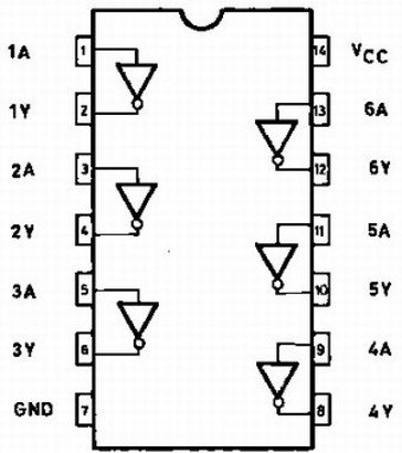
74HCT04 Pinout Diagram
This picture depicts the pinout diagram and the functionality of each pin. 74HCT04 has six NOT gates inside a single chip.

Pin Configuration of 74HCT04 IC
As you can see from the pinout diagram that 74HCT04 has 15 pins. Each Hex inverter has one input and one output pin.

| Pin_Number | Name | Description |
|---|---|---|
| one, three, five, nine, eleven, thirteen | 1A, 2A, 3A, 4A, 5A, 6A | Data Input Pins |
| two, four, six, eight, ten, twelve | 1Y, 2Y, 3Y, 4Y, 5Y, 6Y | Data Output pins |
| 7 | GND | Connect with a ground terminal of power supply |
| 14 | Connect to the positive terminal of the voltage supply
|
Features of 74HCT04 IC
- Hex Inverter IC with a voltage range of 4.5V to 5.5V
- Schmitt triggered inputs and is compatible with the TTL voltage level which allows unlimited rise and fall times.
- Sinks or Sources 4mA at Vcc= 4.5V
- CMOS logic-based with a feature of low power consumption
- Continuous Output Current: ±25mA
- Maximum Propagation Delay is 29 ns
- Min HIGH-level input voltage is 2V
- Max LOW-level input voltage is 0.8V
- Available in SO-14 and TSSOP-14 packages
- Totally Lead-Free & Fully RoHS Compliant
Equivalent options
Other logic gates
74LS00, 74LS08, 74LS85, 74LS86
Where to use 74HCT04 IC?
This IC has six NOT gates having independent inputs and outputs. 74HCT04 can be used in inverting applications or in designing combinational logic circuits. Additionally, it is based on CMOS logic. That’s why it is used in oscillators designing due to their low power consumption. CMOS inverters can be easily interfaced as compared to other logic devices. You can also use this IC in designing square wave oscillators that deploy in generating clock signals. This IC can act as a wave oscillator or buffer depending on how quickly it toggles the output on changing the input signal.
How to Use 74HCT04 IC?
The 74HCT04 IC is very simple to use. You can see from the diagram that it is composed of six NOT gates, each having it’s on input and output. The input pins are supplied with signals. Connect pin 8 to the ground of the circuit and pin 16 with the positive voltage supply.
Before understanding the operation of this IC, lets first look at the behavior of a NOT gate when applied with an input signal A. Let the output be X. Then the Boolean equation for this Not gate would be:
Y = ~A
Truth Table
That means if the input is HIGH, the output will be LOW and vice versa. The truth table and timing diagram for this Not gate would be:
| Input “A” | Output “Y” |
|---|---|
| 0 | 1 |
| 1 | 0 |
The IC 74HCT04 also operates in similar behavior. All the NOT gates inside this IC have the same truth table and timing diagram as shown above.
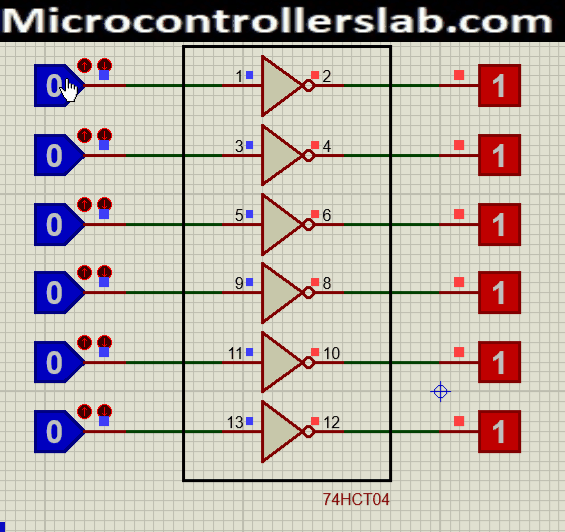
Example Circuits
In this example circuit, we use all six hex inverters. As you can see from the simulation, when input is zero, the output is one and vice versa.
Square Wave Generator Circuit
Propagation Delay 74HCT04 with a Timing diagram
The propagation delay is the most important feature to consider while selecting a gate. If your application needs a high-speed hex inverter, you always refer to a datasheet to find on-time and off-time of the gate. Like other gates, 74HCT04 also has a propagation delay in the order nanoseconds. Propagation delay defines how quickly the input signal will appear on the output. 74HCT04 switching time is around 29ns which is good enough for many applications.

Applications of 74HCT04 IC
The IC 74HCT04 has a huge array of applications. Some of them are:
- For interfacing TTL or NMOS outputs to High−Speed CMOS inputs as a logic level converter.
- Designing general-purpose logic and Combinational Circuits
- It can act as a Wave oscillator or Buffer
- Can be used in the generation of square waves or clock signals
- For handling arithmetic operations
2D Diagram
This diagram shows a two-dimensional physical diagram of DIP package. You need to consider these dimension sizes while designing a PCB.
