74LS04 is a 2 input quadruple 8-bit NOT gate IC. Inverter in logic converters is an electronics device whose basic functions are to invert the incoming logic weather it is HIGH or LOW. They are also known as NOT gates. Inverters are easy to design using NMOS and PMOS transistors. They have only one input and one output. The basic function of transistors is to give the opposite output with respect to input signals. The basic circuit of the NOT gate by use of transistor design is larger in size which is complex and costly as compared to other solutions.
Introduction 74LS04
To solve this problem, we use different ICs that come inverters, the 74LS04 is one of the best IC of 74LS series to use as a transistor. The 74LS04 comes up with six internal inverters. Every inverter uses a single power supply and it can be used individually like each other. The inverter IC comes up in multiple packages, which make its usage in multiple devices. The IC is cheaper and smaller in size. In summary, 74LS04 IC is TTL/CMOS based, it makes IC much reliable to works with other microcontroller TTL devices.
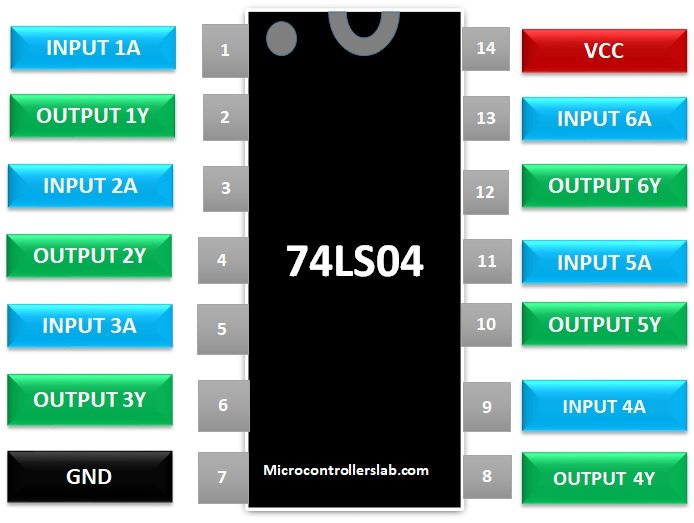
74LS04 Pin Digram
This a pinout diagram of hex NOT gate 74LS04IC.
Other logical gates: 74LS138, 74LS00, 74LS02
74LS04 IC PIN CONFIGURATION Details
This table lists 74ls04 NOT gate details of all pins.
| PINS | DETAIL | |
|---|---|---|
| 1A | Pin 1 | Pin 1 will be used as the input pin for the first inverter. |
| 1Y | Pin 2 | Pin 2 will give the output of the first inverter. |
| 2A | Pin 3 | Pin 3 will be used as the input for the second inverter. |
| 2Y | Pin 4 | Pin 4 will give the output of the second inverter. |
| 3A | Pin 5 | Pin 5 will be used as the input for the third inverter. |
| 3Y | Pin 6 | Pin 6 will give the output of the third inverter. |
| GND | Pin 7 | Pin 7 will be used as a common ground pin when IC will be used with other IC. |
| 4Y | Pin 8 | Pin 8 will give the output of the fourth inverter. |
| 4A | Pin 9 | Pin 9 will use as an input pin for the fourth inverter. |
| 5Y | Pin 10 | Pin 10 will give the output of the fifth inverter. |
| 5A | Pin 11 | Pin 11 will use as an input pin for the fifth inverter. |
| 6Y | Pin 12 | Pin 12 will give the output of the sixth inverter. |
| 6A | Pin 13 | Pin 13 will use as the input pin for the sixth inverter. |
| VCC | Pin 14 | Pin 14 will use as the power pin. It will use to provide the power to the IC, to make it functional. |
74LS04 FEATURES
- 74LS04 gives the output in TTL logic, which makes it workable with any other TTL device and microcontroller.
- Its speed is much faster than a simple transistor-based inverter.
- It comes totally lead-free.
- It comes in multiple packages, SOIC, SOP and PDIP.
- A whole 74LS04 can be used for only one inverter without effecting the other inverter.
SPECIFICATIONS
- The supply voltage range for IC is 4.75V to 5.25. It can be increased up to 7V. More then 7V can make IC burn easily.
- The maximum rise and fall time are faster for most of the controller the other TTL devices. It can rise and fall maximum in 15ns
- The operating voltage of the IC is 0 to 70 degrees.
- IC 74LS04 can draw an output current of 8mA on each gate. It’s the max range, more could harm the IC.
74ls04 RELIABILITY
- The IC cost much less than a single PMOS or CMOS inverter does.
- Its output comes in TTL. Whenever IC needs to be used as TTL. IT can be used easily with any TTL device without usage on any device.
- The single-chip provides four inverters which are smaller in size and faster in speed.
Hex NOT Gate internal
NOT gate is designed by transistors and resistors. The transistor act as a switch and resistor use to change the max current flow. The transistor will be attached to the power supply and resistor. The base of the transistor will act as input and emitter will act as output. Here is the circuit.

There will be two conditions in which the circuit will operate. When input from the “A” is HIGH then the transistor will start flowing the current. The voltage from VCC will start flowing the current from VCC to Ground through the transistor and this will lower the voltages on the A’. Lowering of Voltages will give the LOW state. On the other hand, when we will give the input LOW on the transistor then the transistor will not work. This will allow the power supply to give the full voltages on the output pin.
74LS04 Truth Table
The max voltages will lead the output state HIGH in case of LOW input on the transistor. No matter how the inverter is designed. It will always give the output according to the following pattern. The input will always follow the following truth table on different inputs. All NOT gates following the following formula A = A’.
| INPUT | OUTPUT |
|---|---|
| 0 | 1 |
| 1 | 0 |
How and Where to use 74LS04
The combination of NOT gates cannot make any other gate but a single NOT gate can make other gates by combining with it. If we attach the NOT gate at the start of AND gate then a single AND will become a NAND gate, which will totally invert the outputs. In case of attaching the NOT gate at the start of OR gate, it will convert the OR gate to the NOR gate. Both gates NAND & NOR gate has wide use in making other gates too.
The conversion of NAND and NOR can be done by adding the two not gates on the input, but to reduce the size we add NOT gate at the output which makes us use the one NOT gate only for single gate conversion. The NOT gate only converts the input from HIGH to LOW and LOW to HIGH, but they cannot invert the wave or any signals like transistors can do.
How to use
In 74ls04 IC when we combine the two NOT gates together then it doesn’t have any effect on the output because when the first inverter will convert the state then the second inverter will change the state again. Whenever we use even no of NOT gates in series then there will be no effect on output. The even number of NOT gates will cancel out each other effect. The only odd number will let the change only, even its 1,3 or 5. We will prove this condition in proteus. First, connect the NOT gate with the logic state then check the states it will operate according to the above truth table.


Even Number Example
As we can see the input inverts from 74LS04 NOT gate. Now we will use two NOT gates in series and will analyze the output.

You can see in the image that there is no effect on the output when we apply any input when we connect three 74ls04 NOT gates in series. Then connect the odd no of gates and see the result.
Odd in Series Example

The odd no of gates will act as the same as the single gate does. The series connection will not have any effect on the circuit individually but whenever we want to change the state of single inputs in any other gate than we could connect NOT gate to at the input. Some time multiple NOT gate also used to make proper logic for the circuit. So, we always need to remember whenever the multiple NOT gate will affect the circuit when they are in series with the same wire. If multiple NOT gates attached with the same wire then we can remove them because if they are even in number then remove all of them otherwise use only one, which will minimize the circuit cost and size.
APPLICATIONS 74LS04
- For general Logic conversion
- 74LS04 used as an inverter in servers.
- In the memory unit, the NOT gate is used widely.
- PCs, Notebooks and other smart computers come up with internal NOT gates.
- In digital electronics or any digital system like networking also use gates to invert the states.