CD4052 is a dual 4-channel IC that can be used as both 4:1 multiplexer and 1:4 demultiplexer. It is a CMOS logic-based IC belonging to a CD4000 series of integrated circuits. We can use this IC in both digital and analog applications. In other words, it works for both analog and digital voltage levels. Furthermore, it is controllable through a digital control signal and offer very low resistance in ON state. It is available in a variety of 16-pin packages which includes PDIP, CDIP, SOIC and TSSOP.
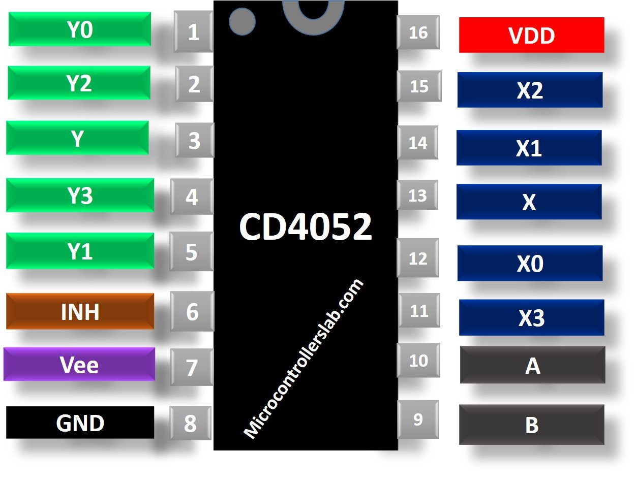
CD4052 Pinout Diagram
This multiplexer IC consists of 16 pins. The picture shows a pinout diagram of CD4052.
Pin Configuration Description
The IC CD4052 has total 16 pins. All the pins, their names, and description are given in the table below.

| Pin Number | Pin Name | Description |
|---|---|---|
| 11, 12, 14, 15 | X0, X1, X2, X3 | Input pins of channel x |
| 1,2,4,5 | Y0, Y1,Y2, Y3 | Input pins of channel y |
| 3, 13 | Y, X | Output for channel X and Y |
| 6 | INH (Enable pin) | For normal operation, it should be connected to ground. |
| 7 | Vss | Negative supply |
| 8 | Vdd | Ground of the circuit |
| 9, Pin10 | A, B | Select pin for channel 0, 1, 2, 3 |
| 15 | Positive Supply |
Where and How to use it?
CD4052 is a dual 4-channel differential multiplexer/demultiplexer IC which has two binary control inputs A and B. In multiplexer mode, it takes 4 inputs from 4 channels and returns the output on channel X, Y. and an inhibit input. The two binary input signals A and B are responsible for selecting channels that which channel should be turned on.
CD4052 IC can also work as a demultiplexer. In this mode, it will take only one input. The select pins A and B will decide that output will be sent to channel 0, 1, 2 or 3. Pin 15 is connected to the power supply and Vss is connected to the ground of the circuit. When inhibit pin is responsible for enabling and disabling of channels. When it is applied with 0 logic, channels are enabled. Channels are disabled no matter what input is applied on select pins when the inhibit pin is applied with logic 1.
CD4052 Working Truth Table
The Truth table showing the effect of the select pins on channel selection is given below:
| INH | A | B | CHANNEL SELECTION |
|---|---|---|---|
| LOW (0) | 0 | 0 | 0 |
| 0 LOW | 1 | 0 | 1 |
| LOW | 0 | 1 | 2 |
| 0 | 1 | 1 | 3 |
| 1 | X | X | None |
How to use CD4052 as a Multiplexer?
In multiplexer mode, it has two channels X, and Y. Each channel has four inputs, such X0 to X3 for channel X, and similarly for Y0 to Y3 for channel Y. Both channels have output pins X and Y respectively. The input pins A, and B are common selection lines for both 4 cross 1 muxes. These selection lines decide which input signal will reflect on output pin.
As you see from this circuit diagram, we are getting output on X and Y pins according to the above table. This is a working circuit diagram. You can play with it in proteus also. As you can see that we give selection line pins A and B are equal to one. According to the selection lines, Multiplexer selects X3 and Y3 input. Therefore, these inputs appear on the output pins such as X and Y.
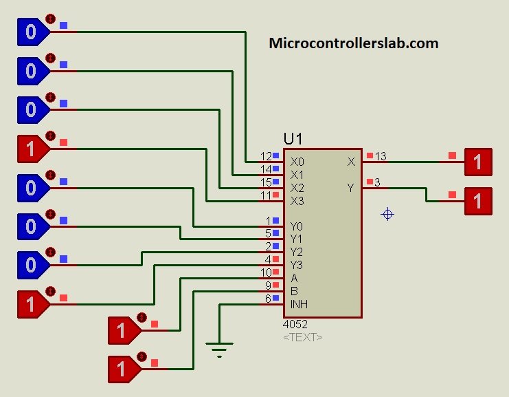
Example Circuit for Multiplexer
This simulation shows a complete working with all possible combinations of A, B inputs. In this example, we use CD4052 as a 4×1 mux. As you can see from the output, the output reflects on X and Y according to the selection line signals.
How to use CD4052 as a Demux?
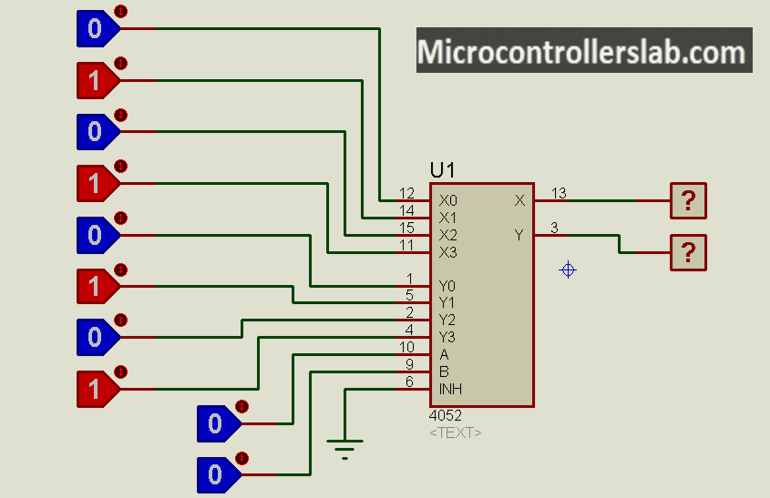
We can also use this ic as a 1×4 multiplexer. We can also call it a decoder. In this configuration, X and Y act as inputs pins. On the other hand, X0-X3 and Y0-Y3 exploit as an output pin for X and Y respectively. Selection pins A and B decide on which pin output should appear. Therefore, output pins will be X1, Y1 or X2,Y2 or X3,Y3 or X0,Y0 depending on digital logic on selected lines that are A and B.
This simulation diagram of the demux depicts the working principle. As you can see from the image, input X=1 and input Y=1 and selection lines A and B both are equal to zero. Therefore, input signals reflect on X0 and Y0. In short, we can change selection line signal values to change the output.

Analog Signals Example
In the last two examples, we see CD4052 working with digital signals only. But mux/demux works perfectly for both digital and analog signals. Therefore, now we will see an example of analog signal selection through a 4×1 multiplexer.
For the demonstration purpose, we design a 4×1 mux example. CD4052 is a dual 4×1 mux/demux ic. But we use only one mux channel in this example. We connect four-level voltage signals with X0 to X4. As you can see the respective analog voltage appears at the output. The voltmeter displays voltage value.

CD4052 Features
- It is a 4-Channel IC that can be used as both 4:1 Multiplexer IC and 1:4 Demultiplexer IC
- It supports both Digital signals and analog signals. The voltage range of Digital signals is 3 V to 20 V and for Analog Signal Levels ≤20 VP-P.
- It has a feature of break before make switching which eliminates the channels overlapping.
- Chip has binary address decoding.
- It is 100% Tested for Quiescent Current at 20 V
- Propagation Delay at 5V is 400ns.
- At 18V, the maximum input current is 1 µA over the full package temperature range and for 25°C, it is 100nA.
- The maximum operating voltage is 20V.
CD4052 Applications
It has numerous applications. Some of them are:
- Analog and Digital Multiplexing and Demultiplexing
- Communication transmission systems for sending multiple signals at one time or sending one signal at multiple carrier channels
- In circuits for Analogue to Digital conversion and Digital to Analogue to conversion
- Signal Gating
- Network switching circuits for example in telephone networks for sending multiple audio signals on a transmission line.
- Programmable Logic circuits
- Arithmetic Logic Units (ALU) are connected to registers inside the Central Processing Unit (CPU). This IC can be used to select the register for storing data or reading data from the register.
- Serial to Parallel Converters
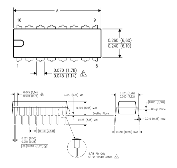
2D Diagram
CD4052 DataSheet
Related Electronics Components:
- ATtiny45 MICROCONTROLLER
- LM317 3-Terminal Adjustable voltage Regulator
- LM1117 800-mA Low-Dropout Linear Regulator
- ULN2003 introduction, pinout, example and features
- CD4022 Divided by 8 Counter IC
- LM1084 5-A Low Dropout Positive Regulator
- TL081/ TL082/TL084 JFET-Input Operational Amplifiers
- UM3561 Three Siren Sound Generator
- MAX7219 8-Digit LED Display Driver
- CD4511 BCD to Seven Segment driver
Please fix up the supply voltage – should be pin 16 and not pin 15