The CD4071 is a quad OR gate IC. In other words, it consists of four OR gates inside the single integrated circuit package. Each OR gate supports two inputs. It is based on CMOS logic. These IC’s are best for use in low power applications.
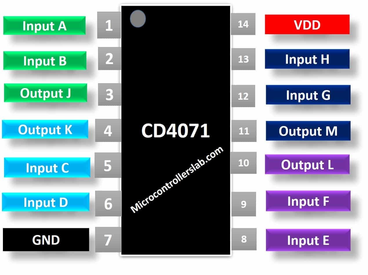
CD4071 Pinout Diagram
This quad 2-input OR gate IC has 14 pins. Three pins are for input and output of each logic gate. We provide a power supply with pin 7(Vss) pin 8 (Vdd). CD4071 is based on CMOS technology. Therefore, it offers a wide range of operating voltage. You can depict the pins of all gates from this pinout diagram.
Pin Configuration Details
| Pin Number | Pin Name | Description |
|---|---|---|
| 1, 2, 5, 6, 8, 9, 12, 13 | A, B, C, D, E, F, G, H | Input pins of OR gates |
| 3, 4, 10, 11 | J, K, L, M | Output pins |
| 7 | Vss | Connect the negative terminal of power supply |
| 14 | Vdd | Connect the positive terminal of a power supply |
CD4071 OR Gate IC Features
- Dual Input IC with 4 OR Gates with an operating voltage range from 3V to 18V
- Fully Static and Medium Speed Operation: with tPHL, tPLH = 60ns (typ) at 10V
- DC input current: ±10mA
- High-Voltage Type (20V Rating)
- Power Dissipation: 500mW
- Maximum propagation delay is 250ns.
- Standard symmetric output
- Minimum logic Low and High voltage @+5V is1.5V and 3.5V
- Maximum Transition Time is 200ns
Equivalent options
- CD4072: 4-input OR gate IC
- CD4075: 3-input OR gate IC
- 74LS32
Other logic gates
74LS00, 74LS02, 74LS08, 74LS86
Where to use CD4071?
This C4071 is used in digital electronics for building Logic level circuits. This IC has 4 OR gates. So, if you require OR operation in an application with lower power consumption and a wide voltage range then you can use this IC. It is also used in designing Encoders and Decoders. You can also use this IC in all those applications where checking of more than events is required. If more than one event occurred, then some operation needs to be done for example checking the temperature or pressure of an industrial plant. You can detect temperature or variable through CD4071. If it exceeds the reference value, then the command will be set to the system to take action.
How to use CD4071 Quad OR Gate?
As this CD4071 has a quad package that’s why it has eight inputs, two for each OR gate. All these inputs are supplied with signals. The pin 7 is connected to the ground of the circuit and pin 14 with the positive power supply. Before understanding the operation of this IC, let us suppose we have an OR gate with two inputs A and B. Then the output Z is given by the following Boolean equation:
Z = A + B
Truth Table
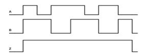
The truth table and timing diagram indicating the behavior of output on changing inputs for CD4071 is given below.
| A | B | Z |
|---|---|---|
| 0 | 0 | 0 |
| 0 | 1 | 1 |
| 1 | 0 | 1 |
| 1 | 1 | 1 |
Timing Diagram
You can observe that the output value will be HIGH when any one of its inputs is HIGH. When both inputs are LOW, the output will be LOW. The IC CD4071 also operates in similar behavior.
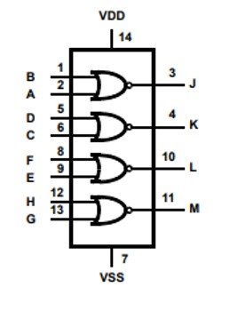
The truth table for all the four OR gates will be same, and their outputs will be given by the following equations:
J = A + B
K = C + D
L = E + F
M = J + H
All these inputs are independent of each other. The functional diagram of this CD4071 is shown below:
Example Circuits
Simple Example
This example demonstrates the working of CD4071. We see all logical input and outputs according to the working principle of the OR gate.
LED Controlling Example
As you can see from this simulation circuit, LED is controllable through both switches such as input A and input B.
CD4071 APPLICATIONS
The IC CD4071 has a huge array of applications in circuits and especially digital electronics. Some of them are:
- In designing basic logic circuits or Alarm circuits for example alarm for a car door system can be designed using this IC.
- Encoders
- Decoders
- We can design Multiplexers of any size and also De-multiplexers


