In this article, we will be uncovering the details of IRF3205. IRF3205 is N Channel HEXFET. HEXFET is the power MOSFET that can be readily found in the TO-220AB package. The operating voltage range of this package is 55 volts & 110 volts. This chip is mainly used in consumer full bridge applications as well as dynamic dv/dt rating. Some other applications like boost convertors, solar inventors, shoppers as well as speed control also use this device. This chip is considered as building block of many electronic application in which the major concern is fast switching as it comes under the ultra-low on resistance devices category that are purely based on advanced process technology. In this article, we will discuss some major points related to IRF3205 to gain deeper insight of this device. Each and everything regarding IRF3205 will be covered in this article i.e. the main features, pin-out, working as well as features. So let’s get started.
Introduction to IRF3205
IRF3205 has been introduced by international rectifier. The main objective of introducing this device is generating extreme low on resistance per silicon area. It is Power MOSFET which is mainly based on the Advance Process Technology and thus it is widely used in applications that require fast switching. IRF3205 is also known as voltage controlled device as it is power MOSFET and it comprises of 3 main terminals known as gate, source and drain. The voltage that is supplied to the gate terminal can be used to handle the other two terminals’ connectivity.
The operating temperature of 175°C as well as low thermal resistance offered by this device makes it an appropriate choice to be used for power dissipation around 50 Watts along with the commercial industrial applications. As compared to other MOSFET, IRF3205 is different as it comes with thick oxide layer at gate terminal and cannot get damaged when exposed to high input voltage while other MOSFET can be damaged whenever they are used in circuits driving high input voltage as they are having thin oxide layer thus affecting the overall performance of that device. This power MOSFET can also be used to operate high power DC motors, industrial applications as well as power tools as this package offers high current ratings. 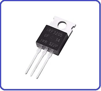
PIN CONFIGURATION of IRF3205
The pin configuration of IRF3205 is as follow:
- Pin 1 is used as gate terminal represented by G and the main task of this pin is to make sure that the flow of current between the source as well as drain channel doesn’t exceed the maximum value.
- Pin 2 is used as drain terminal and is represented by D and electron emission takes place at this terminal.
- Pin 3 is used as source terminal and is represented as S and is used to collect the emitted terminal from the drain.
The flow of current is dependent on the electrons’ movement and the direction of current flow in this device is from drain terminal to the source terminal. The current observed at output terminal is dependent on the voltage that is applied as input to the gate terminal.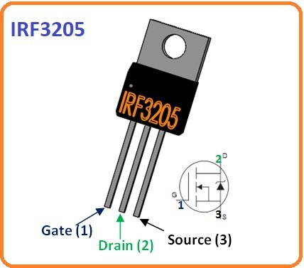
WORKING OF IRF3205
The drain, gate and source terminals of this power MOSFET are analogous to emitter, base and collector terminal present in bipolar junction transistor. The source as well as drain of this power MOSFET is manufactured by using n-type material. The body component of this power MOSFET along with the substrate is manufactured by using p-type material. In order to give the construction of metal oxide semiconductor, an additional layer of silicon oxide is present on the substrate layer. The process of conduction is carried out with the electrons movement thus making this device as unipolar. In order to isolate the gate terminal from the entire body of the device, an insulating layer has to be inserted. The area between the source and drain is known as N-channel.
This N channel is controlled with the help of voltage level that is present at gate terminal. As compared to BJT, the MOSFET use to stay ahead of the curve and the reason behind this is that no input current is needed for controlling a large current amount that is supposed to be present at the other remaining two terminals. If positive voltage is applied to the MOS structure, the charge distribution in device is changed in such a way that the holes present under the oxide layer have to deal with force thus causing the holes to move in downward direction. However you should keep this thing in mind that the bounded negative charges are always connected to the acceptor atoms and they are responsible to flock the depletion region. If the electrons are applied with abundance then they will prove useful while increasing the conductivity of the overall channel thus causing change in the substrate to convert to the N type material.
FEATURES & SPECIFICATIONS OF IRF3205
- The value of VGS i.e. continuous drain current is 110 ampere when 10 volts are applied.
- The amount of pulsed drain current is 390 amperes.
- The power dissipation at the temperature of 25°C is 200 watts.
- The value of linear de-rating factor is 1.3 W/°C.
- The value of gate to source voltage is ± 20 V.
- The avalanche current in this power MOSFET is 62 amperes.
- The amount of repetitive avalanche energy is 0.02 Jdv/dt.
- The value of peak diode recovery i.e. dv/dt is 5 V/ns.
- The soldering temperature as well as operating junction for the time period of 10 seconds is 300 if we assume the length to be 1.6 mm.
- The operating voltage is 175°C.
- Fast switching
- Advanced process technology.
- The package of IRF3205 is TO-220AB
- It is N channel type.
- The rise time value is 110 ns.
- It can be used by combining it with power switching circuits.
- The value of low on resistance is 8 mΩ
- The breakdown voltage of drain to source is 55 volts.
The above mentioned conditions are crucial in execution of the electric circuit. If the stress ratings as well as other rating values are exceeded then they can affect the performance as well as nature of the project. Thus, the ratings should not be applied for long period of time as it affects the device reliability. The most preferred way to use this device is to get hold to these mentioned ratings before you place IRF3205 in the circuit and make sure that the stress conditions as well as operating conditions are met as recommended by the manufacturer.
APPLICATIONS OF IRF3205
IRF3205 is being used in many applications but some of the major applications in which this chip is being widely used are as follow:
- Consumer full bridge
- Commercial as well as industrial applications
- Full bridge
- Fast switching applications
- Push pull
- Choppers
- Speed control
- Boost converters
- Solar inventors
That concludes this article. We hope that each and every point related to IRF3205. However if there is some ambiguity or confusion in this article then are encouraged to ask your question in the comment section below. We will try our best to help you out in best possible way. Your suggestions related to this article are highly appreciated.