In this tutorial, we will discuss LM741 op-amp. LM741 is a general-purpose operational amplifier. Firstly, it has the capability of null- offset adjustment through two pins. Secondly, this op-amp considers as the most suitable option for voltage follower circuits. Because it has no latch-up. Thirdly, the common-mode input voltage range for LM741 is also very high. Therefore, there is no need to use external components for achieving stability. It has internal frequency compensation. Hence, it is fair enough to provide this stability. Moreover, this device has protection against short circuits. In order to null out offset voltage, a small potentiometer can be used. This operational amplifier can operate between ranges of 0-70°C. In short, this op-amp is the best choice for analog circuits.
LM741 Op-Amp Pinout Diagram
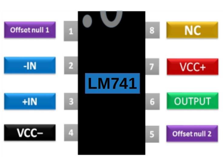
Firstly, LM741 comes as 8 pin DIP and SO8 packages. This diagram shows a pin layout. But the pinout diagram is the same for both packages.
Pin Configuration descriptions
It consists of 8 pins. Two pins are for power supply such as Vcc- and Vcc+. In short, this table lists the descriptions of all pins.
| PINS | Details |
|---|---|
| 1 ( Offset N1) | Offest pin 1 is for external input offset voltage adjustment |
| 2 ( Inverting Input) | Inverting input for applying the inverting input voltage |
| 3 (Non-Inverting Input) | Non- inverting input pin for applying a non-inverting input voltage |
| 4 (-Vcc) | Vcc- is for applying negative DC supply |
| 5 (Offset N2) | Offset Null 2 is for external input offset voltage adjustment |
| 6 (Output) | Output pi is for obtaining output voltage |
| 7 (+Vcc) | Vcc+ is for applying positive DC supply |
| 8 (NC) | This pin is for no connection i.e. it is to be kept open |
LM741 Op-Amp Electrical Features
In this section, we discuss the electrical specifications. One of the main features of this op-amp is overload protection. On top of that, it supports overload protection for inverting and noninverting pins. Unlike other op-amps, it has the following features:
- No latch-up circuit requirement
- Freedom from oscillations
- Available in PDIP, CDIP, and TO99 packages
The operational electrical features of LM741 are:
| Parameters | LM741 |
| Input offset voltage (mV) | 5 |
| Input bias current (nA) | 500 |
| Input offset current (nA) | 200 |
| Input resistance (MΩ) | 2 |
| Large signal voltage gain (V/mV) | 200 |
| Supply current (mA) | 2.8 |
| Output resistance (Ω) | 75 |
| Supply voltage (V) | ±15 |
Where and How to Use LM741 Op-Amp
LM741 is a general-purpose amplifier. We can use it amplification either as inverting or non-inverting. For instance, It can also be used as a
- buffer
- unity gain follower
- comparator
While using the LM741 operational amplifier input signal is either applied at inverting or non-inverting input terminals. These are pin no. 2 or 3. DC supply voltage is applied on pin no. 4 and pin 7.
- We connect the negative potential of the battery to pin 4. After that, connect positive terminal to pin 7.
- After that, it should be noted that +Vcc and –Vcc must be equal in magnitude.
- The maximum values of ±Vcc are shown in the table showing features or datasheet. Similarly, the output voltage is obtained at pin 6.
- Similarly, connects Pin 1 and 5 are used for null offset adjustments. Pin no 8 is segregated as NC which means it is not supposed to be connected anywhere.
Null offset adjustment Circuit
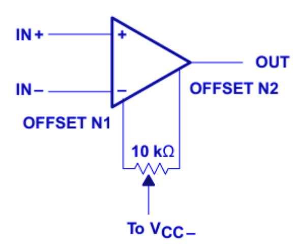
Specific circuit configurations are there to make standard null offset adjustments. This is one of such configurations.
The input offset voltages of OP-AMPs come into action due to the mismatches caused by collector currents, collector gains, collector and emitter resistors. But this mismatch can be removed by making use of offset adjustment pins. In addition, a potentiometer/ variable resistor is connected between the pins 1 and 5 to fine-tune the circuit.
LM741 Circuits Examples
LM741 can be used for the construction of:
- voltage follower
- Unity gain inverting amplifier
- bilateral current source
- AC/DC converter
- instrumentation amplifier
- square wave generator
- voltage comparator
- Power supplies
- oscillators
- half-wave rectifiers
In conclusion, you will see this op-amp in many electronics projects.
Unity Gain Amplifier Example
As we see earlier, one of the uses of OP-AMP is unity gain amplifier or buffer amplifier. The unity gain amplifiers can come up as
- followers
- Inverter
The follower provides a gain of one with output exactly the same as the input. On the other hand, the inverter reverses the polarity of input in addition to unity gain provision. The output resistance of Op-AMP is quite negligible. Hence, this circuit offers as much current according to the requirement of the load.
This diagram shows a circuit of the noninverting unity gain amplifier. In this case, input will be equal to output.
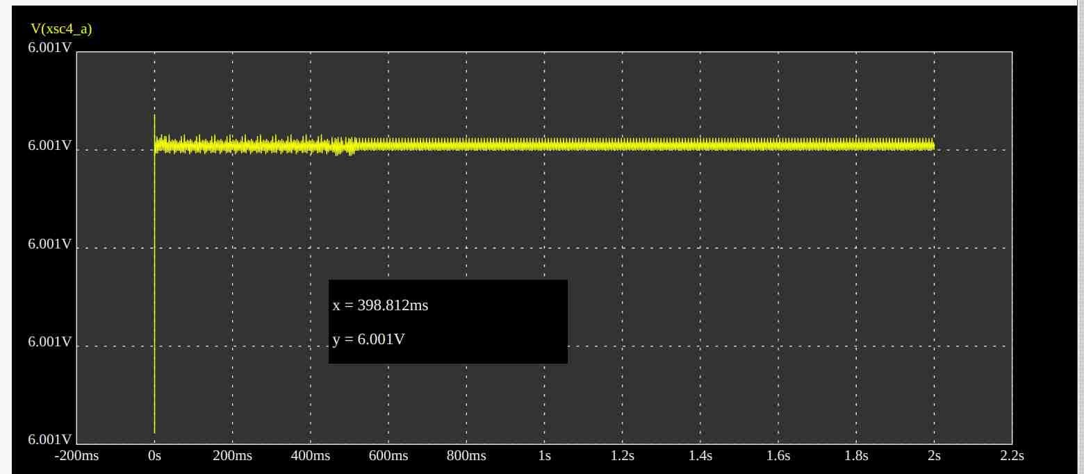
In this circuit, we give an input voltage of 6 volts. After that, we connect a feedback resistor. we get output voltage exactly 6 volts. Because the gain of the amplifier is unity. As a result, the output shows 6 volts on the oscilloscope. According to this equation:
Vout = Vin x Gain
Vout = 6 x 1 = 6 volts   // Because gain=1 and Vin=6 volts
LM741 Square Wave Generator Example
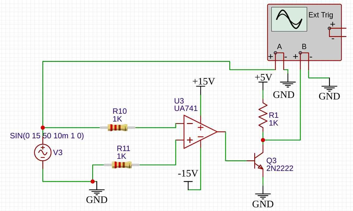
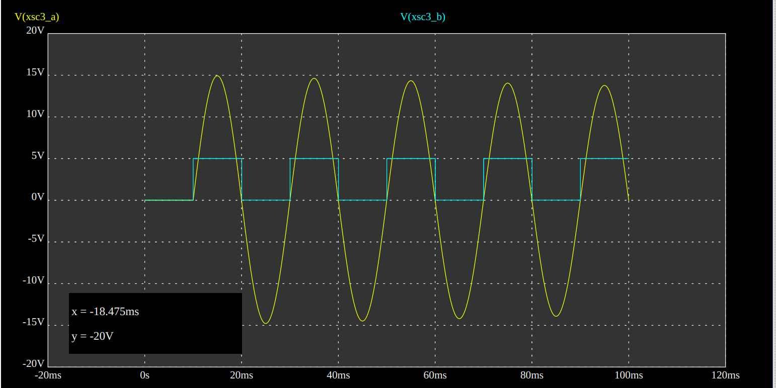
This square wave generator converts an AC sine wave into a square wave. But we can also call it a zero-crossing detection circuit. In short, its main function is to produce a square wave from a sine wave.
In this example, LM741 acts as a comparator. It compares the voltage magnitude of zero voltage reference and sine wave. Whenever a sine wave passes zero voltage level, we will get a square wave at the output. The comparator produces +15 and -15 volts output. But we use edge detection circuits. This edge detection circuit converts op-amp output into a square wave.
Real Electronics Applications
In short, the real-life applications of LM741 are:
- on our mobile phones for AD conversion
- In Audio amplifiers
- Programmable logic controllers
- Video signal conditioning units
- Processors
- Sensor Data Accusation
- digital to analog converters in Phone
- Temperature sensors and controllers
- error amplifiers
- communication circuits
- Mobile phone chargers
- Receivers
- Modulators
- Synthesizers
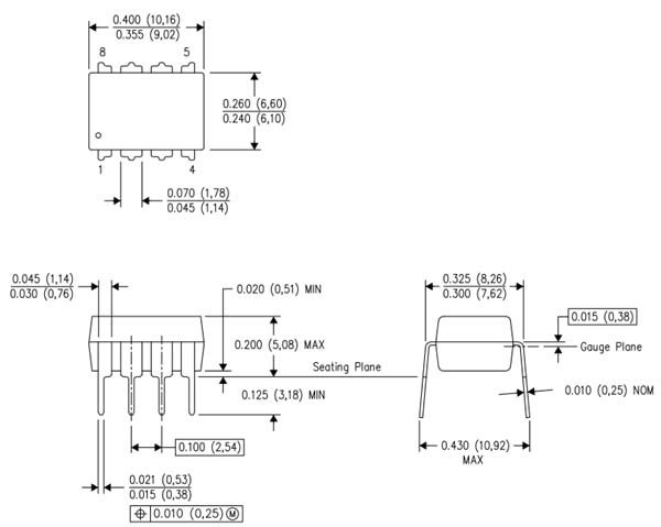
2D physical diagram
This picture shows a 2D physical diagram of a DIP package. But you can download datasheet to check 2D diagram of other packages.
