MCP3008 is a 10-bit Analogue to Digital converter having eight single-ended input channels. It has a 4-wire serial SPI compatible interface that is used to get digital output for all channels. It has an on-board sample and holds circuitry. It provides both analog and digital ground connections which help in noise reduction. It is ideal for use in embedded systems applications.
Additionally, MCP4008 supports 4 differential analog inputs or 8 single-ended inputs. Furthermore, it provides a sampling speed of 200ksps. Most importantly, We can use simple SPI communication to get digital data from all input pins.
Pin Configuration Diagram
As you check from the pinout diagram that it has eight analog channels from CH0-CH7.

Pin Description
The pins description of MCP3008 chip is given below:
Pin#01 to 08: CH0 to CH7
These are the analog inputs for channel 0 to channel 7. These channels can be configured as four single-ended inputs or two pseudo-differential pairs. In pseudo-differential mode, each channel pair are programmed as the IN+ and IN- inputs by sending a serial command string.
Pin#09: DGND
This is the digital ground pin which is linked internally to the digital circuitry of chip.
Pin#10: /SHDN
It is a Chip Select pin. This pin is used to initiate communication with the device by connecting it to low logic level. If it is already low, then it should be pulled to high and then low for initiating communication. When it is pulled to high logic, it will end a conversion.
Pin#11:Din
This is the input pin for serial data.
Pin#12:Dout
It is the serial data output used for SPI communication. On every falling edge of clock signal, data will change, and this converted data is shifted out on this pin.
Pin#13: CLK
It is a serial clock signal used to initiate a conversion and sends each bit out as conversion takes place.
Pin#14: AGND
It is the analog ground pin which is connected internally with analog circuitry. It is connected to the reference voltage.
Pin#15: Vref
It is connected to the reference voltage and is used to determine the range of analog voltage.
Pin#16: VDD
It is the connection for applying a positive voltage to the circuit.
MCP3008 Equivalent
MCP3008 ADC Features
The main features are:
- 8-channel ADC IC with 10-bit resolution and serial SPI interface communication protocol.
- It has programmable analog inputs which can be configured in either single-ended or pseudo-differential modes.
- Operate over a range of 2.7V to 5V.
- The chip employs Successive Approximation (SAR) architecture for ADC conversion.
- The sampling rate is 200ksps for 5V and 75ksps for 2.7V respectively.
- It is based on low power CMOS technology
- The industrial temperature range for this chip is -40°C to +85°C.
- It has a standby current of 5 nA and typical active currents of 320 µA.
Where to use it?
There are some devices like Raspberry pi which don’t have hardware for analog to digital converter and therefore they can’t read analog inputs. So, you need a circuit for this conversion. For such devices, you can use the MCP3008 chip. This chip uses an SPI interface for communication. In Raspberry Pi, only four GPIO pins are required. So, you can get 8 additional analog inputs by using this chip.
Sensors use analog outputs. Therefore, many devices need an ADC converter to read these outputs. The MCP3008 can be used for converting these analog signals into digital signals.
How to use MCP3008?
It consists of a famous SAR ADC architecture technology that contains a built-in sample and holds a capacitor. This architecture performs sampling with a sample/hold capacitor for 1.5 clock cycles on the first rising edge of the clock cycle. After that ADC produces 10-bit digital output depending on the charge value on S/H capacitor
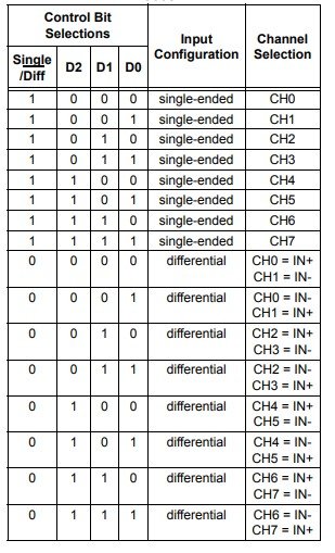
The communication is initiated with the MCP3008 device is accomplished by bringing the CS line low. On the first clock signal (when CS is low and DIN is high), the first bit received will constitute a start bit. This start bit is followed by the SGL/DIFF bit which determines the mode of conversion either single-ended or differential. After that, the next three bits which are D0, D1, and D2 are used to select the channel. On the fourth rising edge of the clock, after the start bit has been received, the sampling of analog inputs will be started.

Reference voltage Selection
Depending on the analog input voltage range we want to connect with analog channels, we can select reference voltage with the help of a reference pin. Lesser the input voltage range and lesser will be LSB size.
LSB Size = Vref / 1024
How to calculate Digital Output?
We can calculate the output reference voltage with the help of this formula.
Digital output= 1024 x Vin / Vef
Configuration Bits
The table is given showing the configuration bits for selecting a mode.
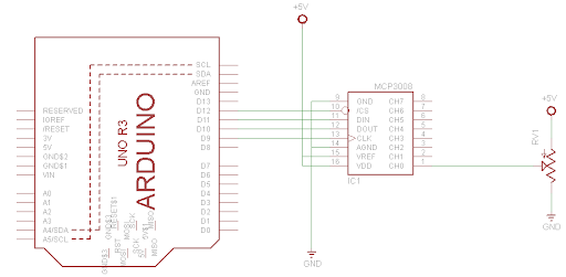
MCP3008 Simple Interfacing Example
A simple diagram is given showing the connections of Arduino with MCP3008 IC.
Applications
- Data acquisition
- Robotics
- Multi-channel data loggers
- instrumentation and measurement
- Controlling servo motors
- Smart sensors