PT8211 is a 16-Bit dual-channel Digital to Analogue converter chip. It is typically a dual-channel DAC that is specifically intended for the applications concerned with digital audio. This DAC chip uses CMOS technology. As the name suggests, it depends on 16-bit and the inner engineering depends on the R-2R resistor ladder network. R-2R ladder is basically an organized set of resistors that converts binary signals to analog.
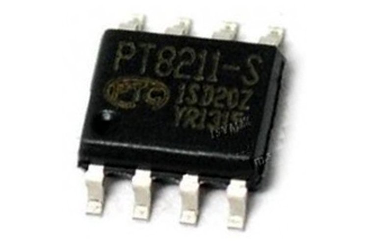
PT8211 DAC Introduction
PT8211 correspondingly improved the execution of timing obligation in a digital serial bus. It consists of a fast switching R-2R network which also supports 8X oversampling audio signal.
It is compatible with TDA1311 in usefulness and also carries an extensive range of test frequencies. The digital timing input format design in PT8211 follows the Least significant bit justified or right justified input data format. 2’s complement and MSB (most significant bit) foremost are the computerized code design of PT8211.
Pinout Diagram
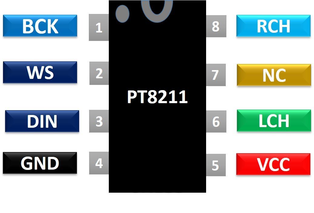
PT8211 DAC is available in 8-pin DIP or SOP. The following figure shows pin configuration diagram.
Pin Configuration
| No. | Name | Function |
|---|---|---|
| 1 | BCK | Serial Bit Clock Input |
| 2 | WS | Word Select Clock Input Pin |
| 3 | DIN | Data Input Pin |
| 4 | GND | Ground |
| 5 | VDD | Positive Power Supply |
| 6 | LCH | Left Channel Input |
| 7 | NC | No Connection |
| 8 | RCH | Right Channel Output |
Features and Specifications of PT8211
- Double audio channel outcome in a single chip
- Uses CMOS technology
- 16-bit vital range
- Suitable for 3.3V but input level
- Low power consumption
- Low total harmonic contortion
- No phase shift within both output channel
- Accessible in 8 pins, DIP or SOP
Alternative options for PT8211 are enumerated below,
- PCM5252
- PCM1789
- PCM1690
Block Diagram of PT8211
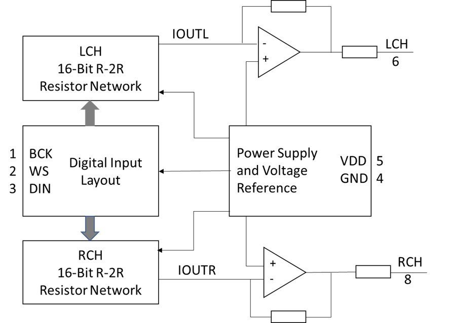
Figure 4 shows block diagram of PT8211
PT8211 DAC Working
The figure below shows the schematic of PT8211 which shows the level interconnection of the DAC. Basic constituents are mandatory to construct it. Few low pass filter associated RC circuits over the output, a couple of op-amps (operational amplifiers), and few GND.
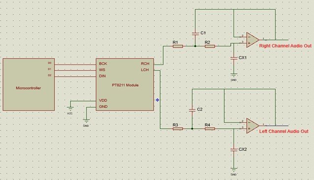
Supplementary low pass filter is located after the analog output of PT8211 to additionally extinguish the remaining noise. The adjustable power supply can be utilized if low noise output is essential for the circuit format.
Timing and Input Signal Format Diagram
Figures below displays the function description of PT8211 in the form of waveforms. Sequential bus input information design of PT8211 is LSBJ. At the rising edge of BCK, each substantial DIN information will be moved to the information register. If the information length is more than 16-Bits then at most the first 16-Bit information from MSB is legitimate, remaining other bits will be shortened. 20MHz could be approached by BCK and upheld to 8x over examining in 48KHz WS clock rate.


The MSB should be the first and DIN information should be in the 2’s complement arrangement. DIN data will be moved to the right input register at the point when the WS clock in the low level. Contrarily, if the WS clock at a high level, DIN data will be moved to the left. 16-Bit R-2R resistor ladder network creates a DAC output. By the means of the cradle operational amplifier, the signal is headed to the RCH/LCH.
Applications of PT8211
- Recorders
- MPEG decoder card
- Multimedia sound card
- Extensive range of audio-related consumer products
- Digital audio equipment
- CD/DVD/MP3 player
2D Model
2D model of PT8211 is shown below which displays the top and side view.
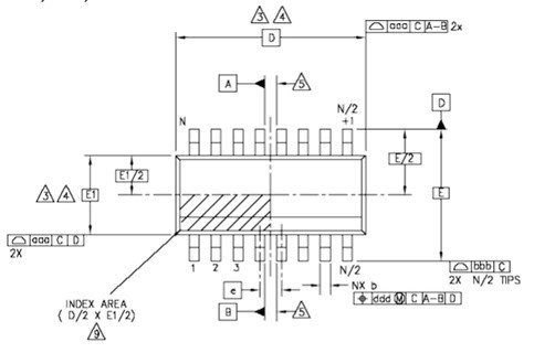
Side view:

In summary, PT8211 DAC is appropriate to use in different sound-related applications where DAC is needed for sound generation or transformation-related work. Subsequently, noise issues are limited as PT8211 provides low total harmonic distortion. Moreover, it is satisfactory for utilizing mobile since it consumes low power.
Related Articles:
very detailed post