74LS90 is a binary decade counter without an automatic reset feature. There multiple kinds of counters which we can use in devices for binary or decimal counting. We discussed a counter 74LS93 IC, which is based on a T-type flip flop. In case of attaching the toggle, flip flops in series we can generate 2n number of binary counters. The IC 74LS93 counts from 0000 to 1111 in binary which is 0 to 15 in decimal. In decimal, we only need 0 to 9 which covers all the possible values of decimal without giving any extra value.
Introduction to 74LS90 decade counter
To solve this issue, we use an IC name 74LS90. The IC contains two MOD counters. One is MOD 2 and the second one is MOD 5 counter. The counter starts counting from 0000 to 1001 and then it resets the value again. The automatic reset makes the counter to start from 0 and end at 9 in decimal. In IC we have four reset pins from which we can enable the counter by activating specific two pins. The IC is TTL based which can work with other TTL based counters and ICs.
74LS90 Pin Configuration
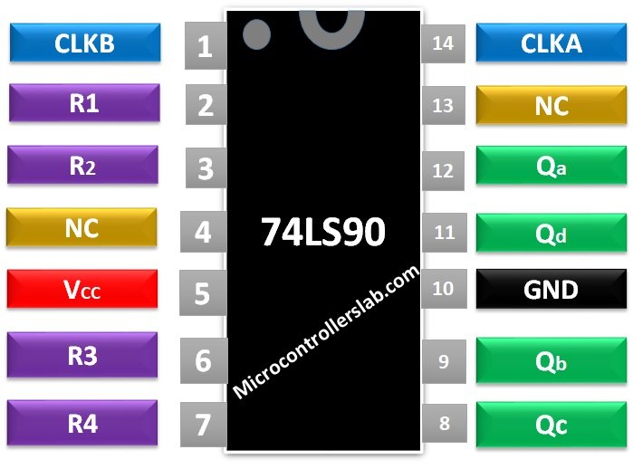
The pinout diagram of the 7490-decade counter is shown here.

| PIN | DETAIL | |
|---|---|---|
| CLKB | Pin 1 | Pin 1 is a clock pulse input of MOD 5 in IC. It’s an active LOW pin to change the state of 3 bits on output. At every high to HIGH to LOW pulse outputs on three bits will be affected. |
| R1 | Pin 2 | Pin 2 is used as a reset pin in the IC. It will show the maximum value on the output. It will use with the Pin 3. |
| R2 | Pin 3 | Pin 3 is also used as a reset pin in the IC. It will show the maximum value on the output. It will use with Pin 2. |
| NC | Pin 4 | Pin 4 has no use it just for balancing the IC to the PCB. It doesn’t matter which it gets connected, it will have no effect on the circuit. |
| VCC | Pin 5 | Pin 5 is a Power input pin used to Power up the IC. |
| R3 | Pin 6 | Pin 6 is used as a reset pin in the IC. It will clear all the outputs with R4. |
| R4 | Pin 7 | Pin 7 is also used as a reset pin. It will clear all the outputs with R3. |
| QC | Pin 8 | Pin 8 is an output pin. It is used to give the second bit of 4-bit output data. |
| QB | Pin 9 | Pin 9 is also an output pin. It is used to give the second LSB (Least Significant Bit) of the 4-bit output data. |
| GND | Pin 10 | Pin 10 is a ground pin. It is used as a common ground with the circuit. |
| QD | Pin 11 | Pin 11 is used as the output pin to give the MSB (Most Significant Bit) of 4-bit output data by the IC. |
| QA | Pin 12 | Pin 12 is also an output used to give LSB of 4-bit output data. |
| NC | Pin 13 | Pin 13 is a no connection pin. It will have no effect on the IC like pin 4. |
| CLKA | Pin 14 | Pin 14 is a clock input pin used to give the clock pulse to the MOD 2 of the IC. |
74LS90 Binary Counter Features
- It is used as a simple counter from 0 – 9.
- The IC has the ability to start from 0 and end at 9 automatically.
- IC can be used any TTL based device and microcontroller due to its TTL output.
- The IC has low power consumption.
- IC comes in multiple packages, PDSO, PDIP, and GDIP
- The IC has internal protection from clamp voltages.
SPECIFICATION
- The Power input range for IC is 4.75 to 5.25.
- The operating temperature range for IC is 0 to 70.
- The input voltages range for IC at HIGH state is 2.0 minimum and the LOW state is 0.7 maximum.
- IC draws output current at HIGH state is -0.4mA and for the LOW state is 8.0mA
- The internal clamp diode protection range is -1.5V.
More information is available in the datasheet:
Other Counters ICs: CD4020, CD4022, CD4060, CD40102, CD4017, CD4026, 74LS93
How 7490 Counter Works?
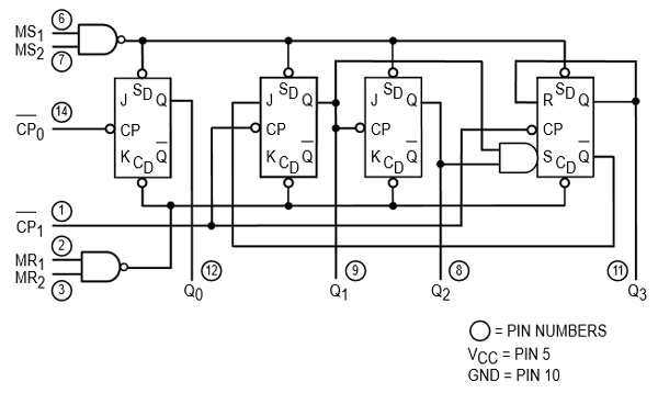
In this section working of 7490 will be explained. The IC has an internal structure of 4 flip flops and the first flip flop is used as MOD 2 and the other three are used as MOD 5. There are two clock pins and they will be used to change the output state. The reset pins are control through AND gate

The IC comes with 4 reset pins, two clock, and 4 output pins. When we are going to use the IC then we need to understand the reset pins first. These four reset pins will be used to control the output. These four reset pins will come up with multiple 16 combinations but in some combinations, there will be fixed output. Here’s the table.
7490 Truth Table
| RESET | OUTPUT | ||||||
|---|---|---|---|---|---|---|---|
| MR1 (R4) | MR2 (R3) | MS1 (R2) | MS2 (R1) | QD | QC | QB | QA |
| H | H | L | X | L | L | L | L |
| H | H | X | L | L | L | L | L |
| X | X | H | H | H | L | L | H |
| L | X | L | X | COUNT | |||
| X | L | X | L | COUNT | |||
| L | X | X | L | COUNT | |||
| X | L | L | X | COUNT |
The second clock pin (Pin 1) will be connected with the LSB of the IC to keep the MOD 2 and MOD 5 is a sequence. The First clock pin (Pin 14) will be used to give the clock input signal to the IC. At every from HIGH to LOW state the output will be affected. But always keep in mind the concept about the reset pins otherwise IC will give some random value or there will be no output. Here the full functional circuit. Whenever we give the pulse the IC will give the output in binary form. Every binary form will represent a decimal number. Here’s the table for every binary number.
| DECIMAL | QD | Qc | QB | QA |
|---|---|---|---|---|
| 0 | 0 | 0 | 0 | 0 |
| 1 | 0 | 0 | 0 | 1 |
| 2 | 0 | 0 | 1 | 0 |
| 3 | 0 | 0 | 1 | 1 |
| 4 | 0 | 1 | 0 | 0 |
| 5 | 0 | 1 | 0 | 1 |
| 6 | 0 | 1 | 1 | 0 |
| 7 | 0 | 1 | 1 | 1 |
| 8 | 1 | 0 | 0 | 0 |
| 9 | 1 | 0 | 0 | 1 |
Counter Example 74LS90
IC 74LS90 can be used as a simple counter but its value always comes in binary. Here we will use the IC as a 0-9 counter and then we will show it on the 7-segment. The IC needs to be used as an IC name 74LS47 to work with 7-segment. The IC will generate the data in binary and 74LS47 will convert the data into a decimal form on the IC. Here’s the circuit and its OUTPUT.

The IC 74LS47 only works with common anode 7-segment that’s why we use the Common anode with IC74LS47. You can also use 74LS48. Here we grounded all the reset pins because we just want to count and we have no intention with the IC to perform any other function. The single IC can only count up to 9 but we can use multiple ICs to count further. In the case of multiple decimal counting, we can use others IC and its method. The IC 74LS90 doesn’t have any special pin to connect the decimals in series or to operate with 7-segment. We always need to come up with self-made solutions with other gates to use the IC as counting more than 9 with 74LS90.
Proteus Simulation
APPLICATIONS 7490 Decade Counter
- The IC can be used for simple binary counting from 0 – 9.
- IC comes up in digital devices with 7-segment.
- IC 74LS90 also use in the servers, networking and Digital Systems.
It was really helpful, thanks
But what does the X mean in truth table?
‘X’ means don’t care. Whatever will be the value either 0 or 1, it will not affect the output.
When we are building the inner circuit of this IC on proteus where will we give the VCC?
Vcc is available by default in proteus. You don’t need to connect.
Can i build a down counter with 74ls90?
le 74LS90 est un compteur synchrone ou asynchrone ?