In every computer system, to acquire data, CPU accesses the hard disk and to do so a lot of time is required. That is why the processes to be executed are put in RAM or the computer’s main memory. The purpose of doing so is that data in the RAM can be retrieved much more faster than any other medium for storage e.g. hard disk drives. RAM is abbreviated as Random-Access Memory. Through RAM, data acquisition is done really fast. It is basically a volatile memory i.e. data is lost as soon as it is shut down. Thus, for it to keep working, constant current flow is required. Then only the data in it can be maintained. Due to this, the data will be erased as soon as the machine will be powered off. RAM has two main types; SRAM (Static Random-Access Memory) and DRAM (Dynamic Random-Access Memory). There are categorized according to the requirement of the refresh cycle.
Basics of SRAM
SRAM stands for Static Random-Access Memory. It is manufactured using the CMOS (Complementary Metal Oxide Semiconductor) technology. It uses 6 transistors. While constructing it, 2 cross-coupled inverters are used. They store data as do flip-flops where extra 2 transistors are used for controlling the access. This scheme is very fast. Moreover, its power consumption is also less. As long as power is being supplied to the machine, SRAM will hold data and will lose it as soon as power will be disconnected, this is similar to the simple RAM.
For the generation of a logic state that is stable, 4 transistors are used i.e. T1, T2, T3 and T4. They are assembled in a cross-connected method. When we are to generate logic state 1, we set node C1 as high and we set C2 as low. Also, T1 and T4 are turned off whereas T2 and T3 are switched on. On the other hand, if we have to set it to logic state 0, the node C1 is set as low and C2 is set high. Similarly, T1 and T4 are switched on, and T2 and T3 are powered off. These two states are stable only when dc voltage is being supplied. If it is interrupted, they will no longer be stable.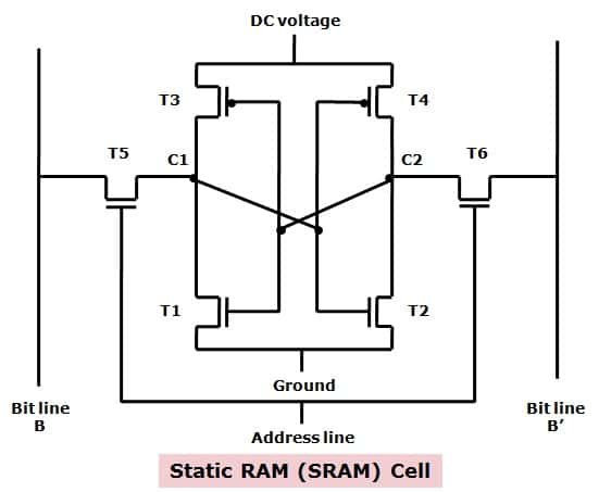
The address line of SRAM is functioned for the switch’s closing and opening and for the control of the 5th and 6th transistors which permits the operations of reading and writing. For the operation of writing, the incoming signal is sent to B bit line and B’ receives its complement. While, for the operation of reading the signal on B line is high and on the B’ line the signal is low when the state of the cell is 1 and the opposite is true when the state is 0.
DRAM BASICS
DRAM stands for Dynamic Random-Access Memory. It is the second type of RAM and is manufactured with the help of transistors and capacitors. The function of capacitor is to store data such that the charged capacitor indicates the value 1 and the discharged capacitor indicated a 0. Capacitor always eventually discharges owing to the fact that charges leak. This phenomenon is shown by the word dynamic. This happens even when power is provided at all times. This is the very reason that DRAM utilizes greater amount of power.
If we have to make the data last for a long period of time, there is a constant need to refresh the data. For this purpose, another circuit is needed. The leaking of charges is such a big problem that it makes DRAM to lose data even when power is being supplied. For greater amount of storage, DRAM is used. It is cheaper as only one transistor is needed for one memory block.
When we have to write or read some sort of data onto or from a cell, we are supposed to activate the address line. In the circuit, the transistor acts as a switch. If it is closed the circuit is complete and the current is flowing and if it is open the circuit is not connected and hence no current is flowing to the address line. When performing the operation of writing, a voltage signal is sent to the bit line, 1 indicates high voltage and 0 indicates that the level of voltage is low. A signal is then used to the address line which enables transferring of the charge to the capacitor.
When we choose the address line for the execution of operation of reading, we turn the transistor on supplying it with the charge stored by the capacitor. It is sent out onto the bit line and to a sense amplifier. Where, sense amplifier is used to specify the logic contained by the cell. i.e. 1 or 2. It is done by the comparison of the current voltage of the capacitor and the reference voltage. On the other hand, for performing the reading operation, capacitor discharging is done by the cells. It is to be restored for completing the operation. DRAM is an analogue device but can still store 2 bits i.e. 0 and 1.
SRAM vs DRAM
- There are a number of differences between SRAM and DRAM. SRAM has a smaller access time as it has an on-chip memory unit whereas DRAM has a larger access time as it has an off-chip memory.
- This marks the difference between their performance. Furthermore, DRAM is used where capacity of storage is larger, and SRAM is used for less storage capacity.
- The example of SRAM includes the cache memory and the example of DRAM is the main memory. DRAM is highly dense, and SRAM is less dense. Plus, SRAM is difficult to construct as it uses a lot of transistors, flipflops and capacitors. While, DRAM only uses a few transistor and capacitor, so its construction is quite simpler.
- DRAM is called so because it uses a capacitor which results in the leakage of current hence the word dynamic. The leakage occurs because of the presence of the dielectric present between the plates of the capacitor. This dielectric separates the conducting plates. Unfortunately, it doesn’t insulate completely.
- As a result, greater power refresh circuitry is required. Whereas in SRAM no such issue arises. Consumption of power is very much high in DRAM than it is in SRAM. The main objective for the operation of SRAM is the change of current direction with the use of switches. On the other hand, DRAM holds the charges.
Comparison Chart
| SRAM | DRAM |
|---|---|
| SRAM is really fast.
| DRAM is slower than SRAM.
|
| There is no need for the refreshing of cycles to make the data retain.
| Cycles are to be continuously refreshed to keep the data.
|
| Its circuitry of SRAM is very complex and hence less time requirement. | Its circuitry is simple and time requirements are larger.
|
| CPU cache is its application
| Main memory is its application.
|
| Its access time is very less
| It has a greater access time.
|
| At a low frequency, SRAM utilizes less power.
| At high frequency, power consumption is comparable.
|
| It uses flipflops.
| It uses capacitors and transistors.
|
| Its density is low.
| Its density is high. |
| It is expensive | It is cheaper |
Conclusion
DRAM is a derivation of the SRAM. DRAM was introduced after SRAM. Its main purpose was to cover the drawbacks of SRAM. This was done by lessening the elements (transistors and capacitors) used for the memory storage of one bit. This speeded down the process greatly, but it is quite cheap, yet it increased the storage capacity. The drawback is that the speed of DRAM is slower and power consumption is greater. Constant refreshing is needed (after milliseconds).