The IC 74LS145 is a TTL based BCD to Decimal decoder used to drive the ten binary outputs on the base of four binary inputs. The IC consist of eight inverter and ten NAND gates which have four inputs. These total eighteen gates come up with a smart circuit that gives ten output through the NAND gates. The inputs go through four NAND gates. The four inputs have a minimum value equal to 0000 and maximum value to 1111.
The IC ensures that it gives HIGH output on invalid inputs and also it gives LOW output on a single output on specific inputs. The IC is compatible to use with any TTL, DTL or and MOS integrated circuits. The IC was designed to use as open collector logic circuits and to use as indicators/drivers for relays. It has low Power dissipation and in the IC clamp diodes control the termination on high speed.
Other equivalents of this IC are SN74LS145, SN54145, SN54LS145, SN74145.
Recommended Components
The following parts are used in this article, along with a generic electronics kit that is handy for building and testing the circuit.
| Component | How it’s used | Buy on Amazon |
|---|---|---|
| 74LS145 BCD-to-decimal decoder | The 74LS145 BCD-to-decimal decoder/driver this article covers. | Check Price |
| Electronic component assortment kit (1390 pcs) | A handy assortment of resistors, capacitors, LEDs, diodes and transistors for building circuits. | Check Price |
| Digital multimeter (AstroAI) | Measures voltage, current, resistance and checks continuity while you build and debug. | Check Price |
| Breadboard | Solderless base for prototyping the circuit. | Check Price |
| Jumper Wires | Make the connections on the breadboard. | Check Price |
As an Amazon Associate we earn from qualifying purchases. Prices and availability are accurate as of the date/time indicated and are subject to change.
SN74LS145 Pinout
The pin diagram of DCB to the decimal decoder is shown here. Different color patterns are used to differentiate input, output and power supply pins.

74LS145 Pin Diagram Details
| PINS | DETAILS | |
|---|---|---|
| Q0 | Pin 1 | Pin 1 to Pin 7 will be used as the first 7 output pins on first 7 inputs. These pins will be in a HIGH state when there is no input or invalid input on the input pins. In case of input that will affect the output, the pin will change the state from LOW to HIGH until the input changed to a new one or invalid. Only one output pin will be LOW at specific input. |
| Q1 | Pin 2 | |
| Q2 | Pin 3 | |
| Q3 | Pin 4 | |
| Q4 | Pin 5 | |
| Q5 | Pin 6 | |
| Q6 | Pin 7 | |
| GND | Pin 8 | Pin 8 will be used as a common ground. The ground of Power supply and other compatible devices ground will be common with Pin 8 to make it usable with IC. |
| Q7 | Pin 9 | Pin 9 to Pin 11 will also be used as an output pin. In these pins, the output will also act like the first seven pins. Only one pin (from first seven and these three pins) will be affected by inputs at a time. |
| Q8 | Pin 10 | |
| Q9 | Pin 11 | |
| P0 | Pin 12 | Pin 12 will be used as the first input pin for the IC 74LS145. |
| P1 | Pin 13 | Pin 13 will be used as a second input pin for the IC 74LS145. |
| P2 | Pin 14 | Pin 14 will be used as the third input pin for the IC 74LS145. |
| P3 | Pin 15 | Pin 15 will be used as the fourth input pin for the IC 74LS145. |
| VCC | Pin 16 | Vcc pin will be used as the power pin to make the IC functional. |
74LS145 Decoder FEATURES
- It can be used for full decoding of all input logic.
- The IC comes up in multiple packages, DIL and SOIC.
- It has a low power consumption of about 35mW.
- All the outputs of the IC will be off for all invalid inputs.
- The IC can be used easily with TTL, DTL, MOS, and any other IC or microcontroller.
- The inputs consist of clamp diodes to control the speed.
- At a single time, the only one output will be LOW others will be HIGH.
- The outputs will mutually exclusive.
- It has a capacity of 1 of 8.
- The outputs will be invalid when input will be above nine.
BCD to Decimal Decoder Specifications
- The voltage range for 74LS145 is 4.5 to 5.25 Volts. The voltage for power supply should not be more than 5.25.
- The temperature range for IC is 0 to 70 degrees.
- The HIGH input state voltage will be 2 and the maximum input voltage for the LOW state will be 0.8.
- The high to low and low to high propagation time is 50ns for IC 74LS145.
- The IC 74LS145 can sink up to 80mA current.
- The input current for the HIGH state is maxed 0.1mA and the LOW state is -0.4mA.
More information on specifications and features available in the datasheet of 74LS145. Download datasheet.
How SN74LS145 Decoder works?
In IC 74LS145 the circuit consists of 8 NOT gates and 10 NAND gates. The two NOT gates are connected with each input and a single NAND gate is connected with each output. Every NAND gate receives four inputs and every output gets inverted from the NAND gate. There will be a total of 11 conditions on which the circuit will operate and we need to understand how each and every input will give the specific output.
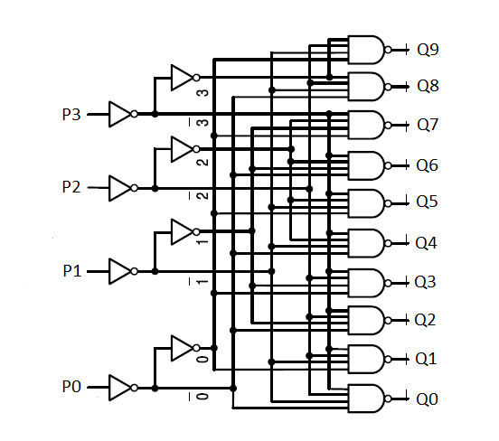
Internal Circuit 74LS145
In IC 74LS145 we have a total of 16 inputs but only from 0000 to 1001 will be able to make the output LOW other will have no effect on the OUTPUT, which makes the state from 0101 to 1111 invalid states. The IC will always follow the following truth table. Every input condition will make the output LOW and those who will not be able to change the output state will be known as invalid states. The invalid state won’t be able to change even a single NAND gate from HIGH to LOW due to the Circuit. The only 10 states will be able to change the outputs which make the circuit 1-10 decoder too.
| INPUTS | OUTPUTS | ||||||||||||
|---|---|---|---|---|---|---|---|---|---|---|---|---|---|
| P3 | P2 | P1 | P0 | Q0 | Q1 | Q2 | Q3 | Q4 | Q5 | Q6 | Q7 | Q8 | Q9 |
| 0 | 0 | 0 | 0 | 0 | 1 | 1 | 1 | 1 | 1 | 1 | 1 | 1 | 1 |
| 0 | 0 | 0 | 1 | 1 | 0 | 1 | 1 | 1 | 1 | 1 | 1 | 1 | 1 |
| 0 | 0 | 1 | 0 | 1 | 1 | 0 | 1 | 1 | 1 | 1 | 1 | 1 | 1 |
| 0 | 0 | 1 | 1 | 1 | 1 | 1 | 0 | 1 | 1 | 1 | 1 | 1 | 1 |
| 0 | 1 | 0 | 0 | 1 | 1 | 1 | 1 | 0 | 1 | 1 | 1 | 1 | 1 |
| 0 | 1 | 0 | 1 | 1 | 1 | 1 | 1 | 1 | 0 | 1 | 1 | 1 | 1 |
| 0 | 1 | 1 | 0 | 1 | 1 | 1 | 1 | 1 | 1 | 0 | 1 | 1 | 1 |
| 0 | 1 | 1 | 1 | 1 | 1 | 1 | 1 | 1 | 1 | 1 | 0 | 1 | 1 |
| 1 | 0 | 0 | 0 | 1 | 1 | 1 | 1 | 1 | 1 | 1 | 1 | 0 | 1 |
| 1 | 0 | 0 | 1 | 1 | 1 | 1 | 1 | 1 | 1 | 1 | 1 | 1 | 0 |
| 1 | 0 | 1 | 0 | 1 | 1 | 1 | 1 | 1 | 1 | 1 | 1 | 1 | 1 |
| 1 | 0 | 1 | 1 | 1 | 1 | 1 | 1 | 1 | 1 | 1 | 1 | 1 | 1 |
| 1 | 1 | 0 | 0 | 1 | 1 | 1 | 1 | 1 | 1 | 1 | 1 | 1 | 1 |
| 1 | 1 | 0 | 1 | 1 | 1 | 1 | 1 | 1 | 1 | 1 | 1 | 1 | 1 |
| 1 | 1 | 1 | 0 | 1 | 1 | 1 | 1 | 1 | 1 | 1 | 1 | 1 | 1 |
| 1 | 1 | 1 | 1 | 1 | 1 | 1 | 1 | 1 | 1 | 1 | 1 | 1 | 1 |
74LS145 decoder Example in Proteus
In this example, we will understand the IC functionality on three states “0000” which is the first state, last state 1001 and the invalid state. First design the IC circuit in the Proteus. Use the logic gates to understand the IC functionality. Design the circuit according to the following diagram:
Figure 3: PROTEUS CIRCUIT
First, give the input as “0000”. You will notice that the input will only make the Q0 active which will make the output LOW and other output will remain HIGH.
Figure 4: WHEN INPUT IS 0000
In another case when the input will be 1001 then Q9 will be LOW and others will remain HIGH
Figure 5: WHEN INPUT IS 1001
In case of values from values between 0000 to 1001, the logic will follow the different paths to make the other gates active but in case of values above 1001, there won’t be any path and outputs will remain HIGH for all the gates.
Figure 6:When input is greater than 1001
The logic states will not active any gate. That is why these states are known as Invalid states. The IC has multiple uses due to its fast speed and usage with another controller. Whenever we will need to use the controller, we will need to use only valid inputs otherwise IC won’t give any output, all will remain HIGH until there’s a valid input.APPLICATIONS S4LS145
- It is used to drive multiple LED lights and for seven-segment displays.
- It also helps to control the incandescent displays.
- IC also helps in gas discharge displays.
- IC helps in to control Florescent displays and LCD displays.
Please note that at the top of the graphic, Output 7, Output 8, and Output 9 are upside down.