74LS166 is an 8-bit shift register digital IC. In cased of 8-bit parallel communication device needs to send the data to the serial receiving device then an 8-bit shift register will be used. There is an IC 74LS166, which has eight parallel data input, one serial input, and one serial output. The IC is made up of almost 77 gates, which has a little complex circuit design. In this shift register IC the data input will be controlled by two clock pins and one load/shift pin. It will be converted only when load/pin will be HIGH and clock pins are giving the HIGH to LOW pulse. SN54/74LS166 comes in multiple packages and is based on TTL logic, which solves almost every hardware requirement and suitable for interfacing with other TTL logic-based devices.
Pinout diagram 74LS166 Shift register
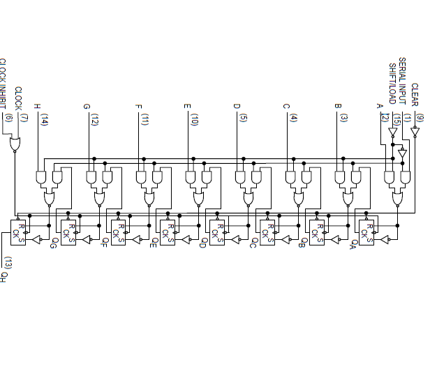
The pin configuration diagram shows different pins for this 74166 shift register IC. Different coloring patterns are used to differentiate input /output pins. This is according to the datasheet.

| PINS | DETAIL | |
|---|---|---|
| SERIAL IN | Pin 1 | Pin 1 is a serial input pin used to input the serial data to the IC. |
| A | Pin 2 | Pin 2 to Pin 5 are the input pins, which are used to input the first 4 bits of 8-bits parallel data. |
| B | Pin 3 | |
| C | Pin 4 | |
| D | Pin 5 | |
| CLOCK INHIBIT | Pin 6 | Pin 6 is a clock inhibit pin; it is used to control the clock pulse signal. It’s an active LOW pin. |
| CLOCK | Pin 7 | Pin 7 is a clock pulse input pin used to change the state of the IC with respect to time. |
| GND | Pin 8 | Pin 8 is a ground pin used as common ground by IC with power supply, receiver and sender device. |
| CLEAR | Pin 9 | Pin 9 is a clear pin used to reset the output data and all internally stored data. |
| E | Pin 10 | After Pin 2 to 5, Pin 10 to 12 are used to give the remaining 3 -bits of the 8-bit parallel data as an input. |
| F | Pin 11 | |
| G | Pin 12 | |
| SERIAL OUT | Pin 13 | Pin 13 is a serial output pin used to receive the converted 8 bit parallel data in a serial form. |
| H | Pin 14 | Pin 14 is used by the LSB of the 8-bit parallel data. |
| SHIFT/LOAD | Pin 15 | Pin 15 is an enable pin of the IC, after activating the enable pin the parallel 8-bit parallel and serial input will be a shift with according to each clock pulse. |
| VCC | Pin 16 | Pin 16 is a power input pin for the IC to make it functional. |
How 74LS166 Works?
IC 74LS166 is made of 77 different kinds of gates, in which some are used as the inverter and some are used as flip flop too. The final circuit of the 74LS166 has 16 pins, which includes 4 control pins in the IC. In the first two pins (7,6), one is used to give the clock pulse to the internal flip flops of the IC and the other pin CLOCK INHIBIT is used to control the clock pulse. If the CLOCK INHIBIT pin is active then the clock pulse will be able to move towards the flip flops otherwise it will have no effect on the IC. In the remaining control pin, the clear pin will be used to clear the data internally and externally. The clear pin (9) will clear all the data from an output pin and internal flipflops, it will act on logical input LOW. In the case of an active clear state, the data of control pins will also be clear. The last control pin, load/Shift is used to enable the data to shift from input pins to the internal flipflops to shift it with each clock pulse.
- Now let’s take a look at data input pins. These pins are total 9 in number and 8 of them are for parallel input, the last one is used for serial input.
- In the case of 8-bit data at parallel input, the parallel data will have preference over serial input and serial data will be shift after the parallel data.
- In SN54/74LS166, the data will be moved in a sequence from latch to latch within the IC, that is why some outputs will depend on the internal flipflop output, but serial output pin will give only the output of the last flip flop of the IC.
74LSLS166 Shift register Truth Table
There is only one output pin and it will give the output according to the following 8-bit shift register Truth Table:
| INPUTS | INTERNAL LATCHES OUTPUT | OUTPUT | ||||||
|---|---|---|---|---|---|---|---|---|
| CLR | SHIFT/LOAD | CLK INHIBIT | CLK | SERIAL | PARALLEL | QA | QB | QH |
| 0 | X | X | X | X | X | L | L | L |
| 1 | X | L | L | X | X | QA0 | QB0 | QH0 |
| 1 | L | L | Pulse | X | a…h | a | b | h |
| 1 | H | L | Pulse | H | X | H | QAn | QGn |
| 1 | H | L | Pulse | L | X | L | QAn | QGn |
| 1 | X | H | Pulse | X | X | QA0 | QB0 | QH0 |
As we can see from the truth table some outputs depend on the internal flip flops but it will only happen in the case of serial input of other functions but in case of parallel input the output will be the same as the parallel input but in series form. It is due to the continuous flow of the data from latch to latch.
Timing diagram 74166
The Internal functionality of the IC can be represented by the following timing diagram:

Applications
- It is used as a module for parallel data to serial data conversion.
- 74LS166 is used to generate the different patterns of an LED.
- In Parallel mouse and keyboards connectors, the IC is used as an interface to communicate between the peripheral and the computer.
Other alternative and Equivalent shift Registers: 74HC595, CD4035,CD4015, CD4014
Example with 74LS166 Shift Register
The IC mostly uses for parallel to serial conversion between devices, but here we will use it to make a small example indicator for the house door. In IC 74LS166 the output will receive only when enable pin will receive high to low pulse. When 8-bits parallel data and serial data has been shifted in a sequence then there won’t be any output until enable (LOAD/SHIFT) pin receives another HIGH to LOW pulse, that is why we are going to use the IC to perform a one-time task for after receiving a single pulse. We will use the buzzer and LED for indication. The circuit will be according to the given diagram and here instead of the door, we will use a push-button, where the open button will represent the closed door and pressed button will represent the open door. Here’s the example circuit diagram:
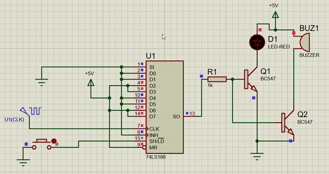
In the above circuit, the buzzer and LED go online twice when we press the button, which is due to the logic input state. In the circuit by changing the logic states the circuit can be converted into continuous buzzer for theft control and another security purpose.
Proteus Simulation
74LS166 Shift Register FEATURES
- 74LS166 allows one-way communication from parallel to serial.
- The direct overriding can be clear from a single pulse.
- The data load asynchronously according to each clock pulse.
- 74LS166 comes in multiple packages, SOP, SOIC and PDIP which solves the requirement for almost every hardware requirement.
- Due to TTL based IC the out and input is TTL based which solves every circuit requirement.
For more features, you can download the datasheet from a link given at the end.
8-bit Shift Register SPECIFICATIONS
- The recommended power input for 74LS166 is 5.25V but IC can operate at a voltage between 4.75 to 5V.
- The power supply current should be a maximum of 38mA.
- The operating temperature range is 0 to 70 but it varies according to a different package.
- The current at the output of the IC is -0.4 at HIGH state and 8.0 at a LOW state.
- The internal protection of Clamp Diode protects up to 0.8V.
- Voltages at the input pins should be Max 2V for HIGH state and 0.7 for the LOW state.