CD4035 is a 4-stage shift register with synchronous parallel inputs to each stage and Serial inputs of J and K_bar to the first stage. It takes data from four parallel inputs, shifts them and then reflects the shifted data on four parallel outputs. The clock input edge makes data shifting. Data shifts on every positive edge of the clock. Each shift register stage consists of D Flip Flops connected in series with each other.
CD4035 Pinout diagram
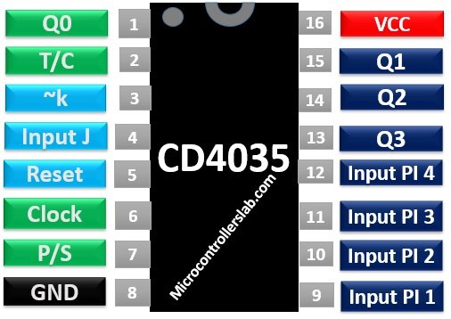
Pin Configuration Details
This IC has 16 pins. Their description is given in the table below.
| Pin Number | Pin Name | Description |
|---|---|---|
| 1, 13, 14, 15 | Q0, Q1, Q2, Q3 | Outputs |
| 2 | T/C (True/Complement) | When this control input is Low, the complement of the data in the register is displayed on the output. Otherwise, the true value will reflect on the output pins. |
| 3, 4 | J, ~k | Serial Inputs |
| 5 | R (Reset) | Reset pin is used to reset the output values to 0. |
| 6 | C (Clock) | Clock input puls |
| 7 | P/S (Parallel/Serial Control) | It enables the parallel or serial entry of inputs into the register. |
| 8 | Vss | Ground of the circuit |
| 9, 10, 11, 12 | Inputs PI-1 to PI-4 | Parallel data inputs |
| 16 | Vdd | Positive power supply |
CD4035 Features
- 4-bit parallel In/ parallel-out clocked Shift register
- 4 synchronous parallel inputs, asynchronous T/C control input and an asynchronous common reset input
- Operating Voltage: 3V to 18V
- Master-slave configuration with static flip flop operation
- Buffered inputs and outputs
- Propagation Delay Time: 500 ns
- Quiescent current specified up to 20V
- High speed: 12 MHz (Typ.) at VDD = 10 V
Alternative shift register ICs
Where to use CD4035?
This IC is used for data storage or shifting of data as it is a shift register IC. CD4035 has 2 serial inputs along with for parallel inputs. This feature enables this IC to convert the serial data into parallel data. So, you can also use this IC in converting between serial and parallel interfaces. This IC is useful in many circuits for generating time delays, data storage, data transfer, manipulation and many more tasks like these can be performed through this IC.
How to use it?
The purpose of shift registers is to shift the data. The operation of this IC is simple. It has four parallel data inputs and two serial inputs. When P/S control input is low, the register is in the serial mode and all the register stages are connected in a serial D flip flop configuration. When the control input is High, the register is in parallel mode. This input pin is responsible for deciding parallel or serial entry of data.
Internal Logic Diagram
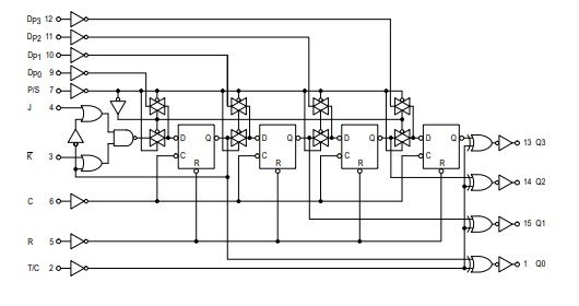
On the positive edge of a clock, data enters the register in either parallel mode or serial mode depending upon the P/S input. Serial inputs are used in counting and sequence generation applications. They are connected to the first stage of registers. The T/C control input complements the data in the register when it is applied with a low logic level. An asynchronous reset input is provided to reset the output value to 0.
Truth Table
The truth table of this IC is given below. It shows the effect of change in inputs on the output when parallel/serial control input is 0 and true/complement input is 1.
| Inputs | Output | |||
|---|---|---|---|---|
| C | J | R | ||
| 0 | 0 | 0 | 0 | |
| 0 | 1 | 0 | Q0(n-1) | |
| 1 | 0 | 0 | (n-1) | |
| 1 | 1 | 0 | 1 | |
| X | X | 0 | Q0(n-1) | |
| X | X | X | 1 | 0 |
Example Circuits
Three-phase signal generator using CD4035
This example circuit generates 3 phase signal using this parallel in/parallel-out shift register. We can use this circuit example to variable frequency driver for three-phase induction motor. This example circuit consists of two NOT gates CD4049 and a CD4035 shift register.
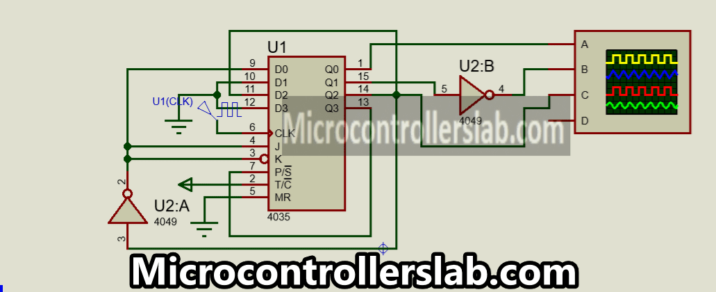
It will generate three PWM signals that you can use to drive three-phase H-bridge circuits. The output of PWM signals depends on the frequency of the input clock signal. The frequency of the input clock signal for CD4035 should be six times the frequency of your required output signal.
For instance, if you want a frequency of output signals 50Hz, the frequency of the clock should be 50×6=300Hz. Therefore, the formula for output frequency is:
fo= fin/6
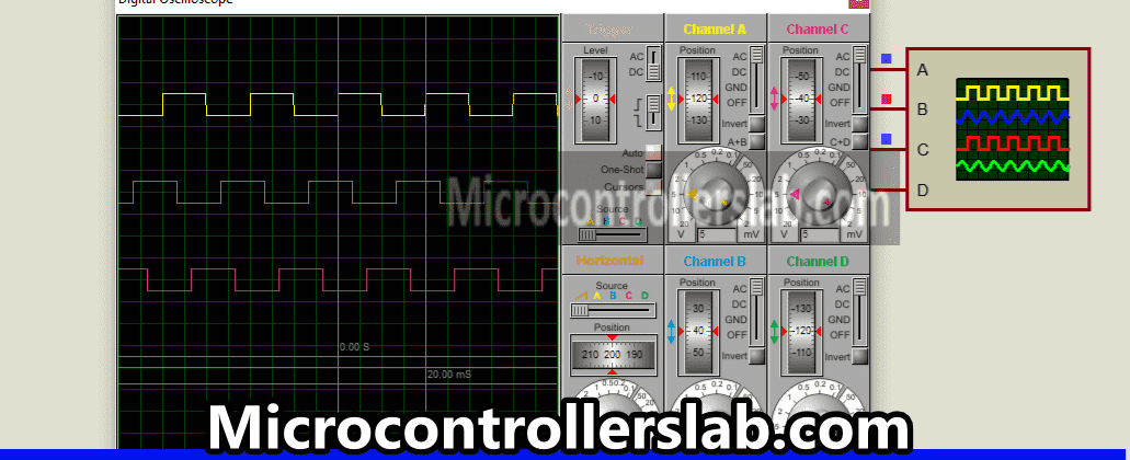
Where fo is output frequency and fin is an input clock frequency. This output diagram shows a 50Hz signal PWM for a three-phase ac motor drive.
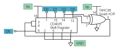
Linear feedback shift register using CD4035
This is an example circuit of a linear feedback shift register. One additional component is the XOR gate IC.
CD4035 Applications
The CD4035 IC is commonly used in:
- up/ down Johnson or ring counters
- sample and hold registers and Control circuits.
- for left shifting and right shifting of data
- conversion of parallel and serial interfaces
- sequence generation, frequency, and phase comparators
- up/ down Johnson or ring counters
- pseudo-random code generation
2D Diagram
Datasheet
Other Electronics components