Full Adder implementation using VHDL on basys 2 FPGA board. In this tutorial you will learn how to implement full adder on basys 2 FPGA board and how to write VHDL code of full adder using two half adders. VHDL code for full adder will be given in later part of this article. First I will explain what full adder is and how full adder works? And how to understand working of single bit full adder and then I will guide you step by step how to implement full adder on Basys 2 FPGA board. Full adder has 3 inputs and 2 outputs. Sum up all the three inputs and outputs the sum. Usually cascaded together to form large adders.
you may also interested to read:
VHDL code of full adder with test bench
library IEEE;

use IEEE.STD_LOGIC_1164.ALL;

use IEEE.numeric_std.all;

use std.textio.all;

use ieee.std_logic_textio.all;

entity test_Full_Adder_2 is

end;

architecture test of test_Full_Adder_2 is

component Full_Adder_2

port (

                S : out std_logic;

                C_out: out std_logic;

                x : in std_logic;

                y : in std_logic;

                C_in : in std_logic);

end component;

signal x_in : std_logic;

signal y_in  : std_logic;

signal c_in  : std_logic;

signal s_out : std_logic;

signal c_out : std_logic;

signal s_expected : std_logic;

signal c_out_expected : std_logic;

signal inputs    : std_logic_vector(2 downto 0);

signal outputs   : std_logic_vector(1 downto 0);

begin

dev_to_test:     Full_Adder_2 port map (

S => s_out, C_out => c_out,

x => x_in, y => y_in, C_in => c_in);

 -- create test outputs

                inputs <= c_in & y_in & x_in;

                c_out_expected <= outputs(1);

                s_expected <= outputs(0);


                expected_proc : process(inputs)

                                begin

                                                case inputs is

                                                when "000" => outputs <= "00";

                                                when "001" => outputs <= "01";

                                                when "010" => outputs <= "01";

                                                when "011" => outputs <= "10";

                                                when "100" => outputs <= "01";

                                                when "101" => outputs <= "10";

                                                when "110" => outputs <= "10";

                                                when "111" => outputs <= "11";

                                                when others => outputs <= (others => 'X');

                                                end case;

                                end process expected_proc;
                                stimulus : process

                                -- variables for test bench

                                variable ErrCnt  : integer := 0;

                                variable WriteBuf : line ;


                                begin

                                                for i in std_logic range '0' to '1' loop

                                                                c_in <= i;

                                                                for j in std_logic range '0' to '1' loop

                                                                                y_in <= j;

                                                                                for k in std_logic range '0' to '1' loop

                                                                                                x_in <= k;


                                                                                                wait for 10 ns;

                                                                                                if (c_out_expected /= c_out) then

                                                                                                write(WriteBuf, string'("ERROR FA test failed at c_out: x = "));

                                                                                                write(WriteBuf, x_in); write(WriteBuf, string'(", y = "));

                                                                                                write(WriteBuf, y_in); write(WriteBuf, string'(", c_in = "));

                                                                                                write(WriteBuf, c_in);


                                                                                                writeline(Output, WriteBuf);

                                                                                                ErrCnt := ErrCnt+1;


                                                                                                end if;


                                                                                                if(s_expected /= s_out) then

                                                                                                write(WriteBuf, string'("ERROR FA test failed at sum: x = "));

                                                                                                write(WriteBuf, x_in); write(WriteBuf, string'(", y = "));

                                                                                                write(WriteBuf, y_in); write(WriteBuf, string'(", c_in = "));

                                                                                                write (WriteBuf, c_in);


                                                                                                writeline(Output, WriteBuf);

                                                                                                ErrCnt := ErrCnt+1;

                                                                                end if;

                                                                end loop; -- k

                                                end loop;  -- j

                                end loop; -- i


                                if (ErrCnt = 0) then

                                                report "SUCCESS! Full Adder Test Completed.";

                                else

                                                report "The Full Adder is broken." severity warning;

                                end if;

                end process stimulus;
Modelsim Simulation
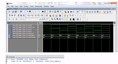
Here is a screenshot of how your ModelSim simulation looks like. Not the transcript in the lower left corner as an indication of successful simulation.
Tasks
Here is a list of tasks you need to do in order to complete this task on full adder implementation with basys 2 and basys 3 board.
- You have to create a modelsim project and successfully simulate a full adder.
- Create a project in Xilinx ISE and successfully create a (*.bit) file.
- Program your BASYS 2 board using the (*.bit) file that you have already created.
UCF File pin mapping
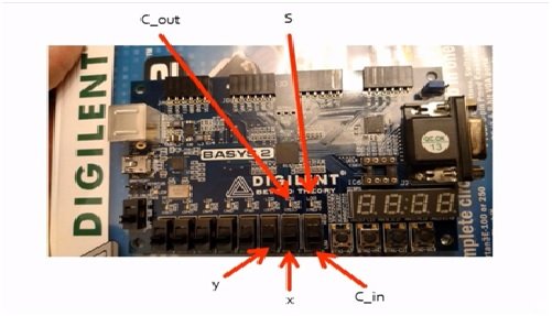
Using UCF file given to you here are the locations of all the different entity port members. You will be targeting inputs Y, X and C_in and verifying that you get correct outputs C_out and S.
Outcomes
Here are the outcome following the completion of lab 1.
- Learn how to create a ModelSim project and simulate a HDL Design.
- Understand how to create a Xilinx ISE and program a FPGA development board based off a VHDL design file.
- Become more familiar with Altera’s ModelSim simulation software and Xilinix’s ISE software.
BASYS 3 Full Adder Demonstration
- Here we are going to demonstrate how to do full adder lab in BASYS 3 full adder. First of all when you open VIVADO, click on create new project.
- Then this window appears. Click on next.
- Then, write the project name in option of project. I have put project name Project_Adder_2. Also put check on create new subdirectory option, it contains all your projects. It makes easier to maintain all your projects. Then click on next.
- Select RTL Project. Everything you will be doing in this course will be using RTL Project. Click on Next.
- Here we can add sources. Here you can add your full adder design file. In target language option write VHDL and in simulator languages select mixed. Then click on next.
- Then, we have to add if we have any IP property but we don’t have so click on next.
- So, we don’t have any constraints we can add it later, move next.
- Now, this window appears. This is the FPGA and it is located on BASYS 3 Full Adder. We have certain boards. Click on boards.
- This Window appears on clicking boards. It gives us 3 different boards Zedboards, Artix-7 Evaluation Platform and ZYNQ.
- We are using BASYS 3, so select on parts. In product category, select all. In family, select Artix-7 and in package select cpg236. In speed grade, select -1. It gives us 3 parts option on screen xc7a15, xc7a35, xc7a50. It gives us all the resources. In part 2 we have 236 I/O, 90DSPs, so on and so far. By moving the cursor you can see all the different characteristics of every part. Then select Next.
- Here you have everything that will be added in your project. Then, click on finish.
- Then it starts creating your project, all the files you need.
- This window appears. You can see we have project summary. We have any file, we have synthesized anything is there.
- First of all what we are going to do is add design sources. For that right click on design sources and then click on add sources.
- Then click on 2nd option i.e. add or create design sources and then click next.
- This is where we are going to find Full Adder 2 VHDL Files.
- Then go to the location of your files. My location is desktop, lab 1 folder, go to BASYS 3 and then go full adder 2 and click ok.
- Make sure, you have copy sources into project option checked that will edit the actual file. Then select finish.
- Then you can see full adder 2 in our design sources files.
- So, if you double click on Full adder 2, you can see a window on right side that allows to edit your file. We can make changes in our sources file by editing it in this window.
- Next, we are going to do is add our constraints file. This marks the port in full adder 2.
- Right click on constraints and then click on add sources.
- This time, we are going to select first option add or create constraints and then click on next.
- Then click on add files.
- Then go into the same directory from where we added full adder 2. At the bottom, in option files of types select constraint files and you get a constraint file named full adder 2 xdc. Click on Ok. Then check copy constraint files into project and select finish.
- Right now, we have everything needed to create new project. On the left side we have project manager, IP integrator, Simulation, RTL Analysis, Synthesis, Implementation and Program and Debug.
- Now, click on Run Synthesis, 2nd option in synthesis.
- In synthesize, make sure all the VHDL code we have is understandable by the compiler and it’s going on. You can notice in the top right corner, its running synthesis design.
- We can go ahead in select log. This is where everything happens.
- It also tells us how much time it is taking to run. Then there is a message that the synthesis is completed. The nect thing we are going to do is Run Implementation. We select OK here.
- Then we are going to go in implementation, the option above log. This is where we are going to run all the signals in the actual FPGA. If you have any problems in your design if you missed out something we come into line now this is where it will throw a warning or an error telling you that your design is wrong or anything else you have.
- So, once you get past the implementation stage we will go ahead and generate bitstream which is what we’re actually placed on here. E.J. so where it is basically is what it has to run. When you have designs that are more complex it may take hours to do. If you have super complex design, it may take three or four hours for this to run.
- At times, it may take overnight to run.
- Now, we are not going to open them, we are going to generate bitstream since we have no errors.
- Go ahead and then click OK.
- You can also go on left hand side of your screen where you can find a generate bitstream button.
- With the basic 3D FPGA we have two megabytes bitstream. Whatever project you do, you always have same bitstream size. We have a flatter or we have 7 segment display. So, we have a two megabyte bitstream file. So, it’s running through an OK. Now, open the harbor manager using the reports and see your resource utilization.
- Now, select the open harbor manager.
- This is what we are going to use actual program the basis for. Now, connect the freebasing stewpot. Open new target. Is you have already connected to your bases seaboard you can select recent targets and it should be an option for starting your day. But what we will do is open a new target and bring upto a wizard that will guide you. Then select Next.
- We want to do local server that’s because we are at the basis the board is connect to the PC. We are actually running here on a machine we are not running on a remote server.
- Then select Next, it goes through a check and see what devices it can connect to.
- You can see that the device here is Xilinx thesea digital and has got a specific code on it.
- If you leave everything with default this X-C seven eight thirty five t that is the actual FPGA. Then we can go ahead and finish.
- Now, we are connected to basic 3 board the hardware manager.
- Then, select program device and it gives us the option of X-C 70, 30, 40 that’s the FPGA is located on the basis of board on which it works.
- Then, we are going to select Bitstream file and the default is enough water to project and created its own directory structure so that you can see this one or two project that is called Dot runs.

Now you can test it. We have c_out and s as the first two entities in port. If I push one switch up I have got a binary one out which tells that we have got single output.
BASYS 2 Full Adder Demonstration
You have got three different inputs here x y in your scene and two outputs. Three bits are added up and the output is given centrally. If I have all of the inputs as zeros there will not be any output. If I put one on I have a one hour mean that the output is wonderful at for addition of all these inputs is one of two tool. I get a binary 2 0 1 0 which is represented by LTD’s right. If I put another 1 on all the three are inputs and I get output 1 1 which is a binary 3.
BASYS 2 Full Adder Solution
- Here we have all the steps needed to complete the lab 1.
- There is a zip file you download. Open that file ans you will all the content of lab 1.
- This is a complete VHDL file provided in that folder. If you have to do any code editing in it, you can do otherwise move on.
- You can also find lab 1 tasks in your folder. If you open that you can see the list of tasks.
- Open up your model Semb.
- Locate your lab 1 folder.
- Create a library to work out for.
- Go to tools, TCL and Execute Macro.
- See simulation on your screen.
- Go ahead and close that.
- Open up the ISC Project.
- Open new project wizard and locate lab 1 folder.
- Then specify the target device.
- Go ahead and Finish the Wizard.
