Optimized Design and simulations of D-Flip Flop using DSCH3, Xilinx ISE & Microwind: In this article we have studied the simulation, verilog verification and physical layout design of D Flip-Flops using different simulation softwares. Flip Flop is basically a device which maintains its state until positive or negative edge of clock triggered. The main objective of this paper is study and analyze different types of Flip flops and design their physical layouts. DSCH is used for logical simulation of different types of D Flip-Flops and Hardware description language verilog is also used for logical verification. Xilinx ISE is used to write verilog code and simulate results. We have verified the output of different types of Flip flops using these simulation softwares. At the end layout of different types of D Flip-Flops is designed using microwind software. We have tried to optimize our layouts as maximum as possible.
So in this paper first of all we will analyze the implementation of D-flip flop in DSCH software. we will implement following types of D-flip flop in DSCH simulation software first. In sequential digital circuits Latches and flip flop are two very common types of circuits that are used. The basic difference between latches and flip flops is that latches are asynchronous which means they change the data as soon as the input of the circuits changes, whereas flip flops are synchronous or clock operated. Flip flops store data and update it depending upon the input clock. They are positive edge triggered or negative edge triggered of clock.
In this project we are going to implement different circuit configurations of D-flip flop which is most commonly used flip flop in digital circuits. For the implantation of circuits DSCH3 software is selected which is easy to use and give accurate results.
1. Master Slave D type Flip Flop
The basic D flip flop design is master slave type. In this configuration two oppositely phased latches are used, one acts as master whereas other as slave. For synchronization purposes a clock is used. The master latch allows the D input when clock Φ=0 and M1 acts as close switch. At the meanwhile nmos M3 and M4 are open. When the clock makes transition from 0 to 1 then M3 and M4 starts conducting and the bit of input appears at the output. The same configuration is implemented in DSCH3 as shown in figure 2 and 3. The output is when input is one with respect to clock.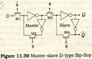
Figure 2.Master Slave DFF with input zero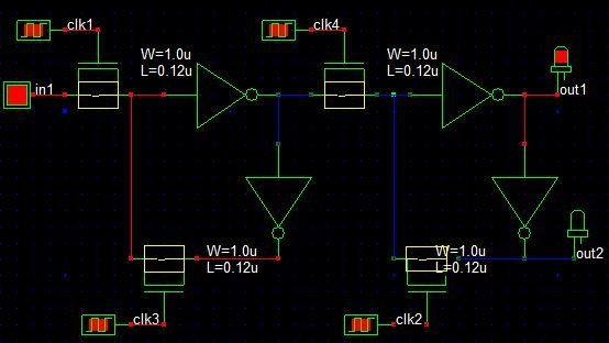
Figure 3.Master slave DFF with input 1
2. Alternate Circuit for Master Slave DFF
In CMOS circuits delay is an important factor. Depending upon this factor there is an alternate circuit for master slave DFF. In this circuit the data path for the input D to output Q is through 4 not gates instead of 2. As delay depends on the number of gates in the path, so in this circuit the delay is greater as compare to first circuit.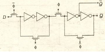
Figure 4.Alternate circuit for Master Slave DFF
Figure 5.Alternate Master slave DFF with input=0
Figure 6.Alternate Master Slave DFF with input=1
3. DFF with Assert low Clear and Set Control inputs
In this new configuration a Set and Clear capabilities are added. A clear input signal is used to clear the input bit stored in the DFF. This is achieved by NAND2 gates by replacing inverters in the original circuit with NAND gates. When the clear =0 then the output Q=0,it forces the master logic to be 1 which is inverted by the slave at the output. When clear=1 then the circuit acts as normal DFF. Its circuit and DSCH3 implementation is show in figure 7 and 8 respectively.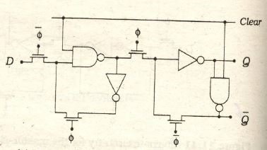
Figure 7.DFF with clear control
Figure 8.DFF with Clear control in DSCH3
Another configuration is possible with both Clear and SET control signals. SET is actually a control which is used to directly set the output to 1whenever needed. When SET=1 then circuit behaves as normal DFF and when SET=0 then it forces the output Q=0. Here one important condition is that both SET and Clear can’t be 0 at the same time otherwise it gives Q= Q’s complement. This configuration is achieved by using NAND2 gates instead of not gates.
Figure 9.DFF with SET/CLEAR Control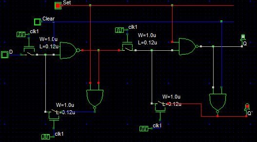
Figure 10.DFF normal operation SET=1
Figure 11.DFF forced to 1 when SET=0
4. DFF Modified to T-Flip Flop using Feedback
A toggle flip flop (T-flip flop) can be created from D-flip flop by introducing a feedback loop in normal DFF circuit. This feedback is provided by connecting Q` to input D as shown in figure 12. An assert Set is used to initially forced the circuit to give 1 whenever needed.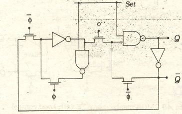
Figure 12.TFF using DFF with feedback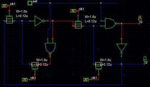
Figure 13.TFF using DFF with feedback in DSCH3
5. D-Flip Flop with LOAD Control
In D flip flop storage of data for an arbitrary number of clock cycles can be obtained by introducing a new control input LOAD to the basic CMOS master slave configuration of D-flip flop. A simple condition is used at the M1 FET. According to this new data will be loaded from the input whenever this condition is 1. For storage purpose a capacitor is used at master latch. Whenever master latch gets open at Φ=0 and load=0 then capacitor Cs stores the charge to maintain the voltage. But due to charge leakage this becomes a Quasi-dynamic circuit which may results in longer delays.
Figure 14.D-flip flop with load control
Figure 15.D-flip flop with load control in DSCH3 when load=1
Figure 16.D-flip flop with load control in DSCH3 when load=1 & input D=1
Simulation and verification of D-Flip Flops in in xilinx ise
For analysis of HDL designs of D flip flops, we pick Xilinx ISE (Integrated Synthesis Environment). This software tool produced by Xilinx for synthesis and analysis of HDL designs, enabling the developer to synthesize (“compile”) their designs, perform timing analysis, examine RTL diagrams, simulate a design’s reaction to different stimuli, and configure the target device with the programmer.
A flip flop differ from a latch in that it is non transparent. The output of a D Flip-Flop always follows the input data. The output of the Flip-Flop may be clocked. If the output is clocked then the D Flip-Flop is synchronous D Flip-Flop. Synchronous D Flip-Flop, thus, has output which is synchronized with the either the rising edge or the falling edge of the input clock pulse. The block diagram of synchronous D Flip-Flop is shown in Figure 17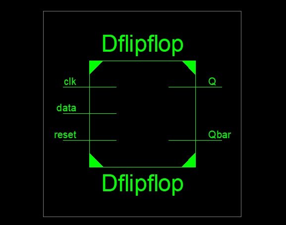
Figure 17: Block Diagram of D Flip Flop
Truth table of synchronous D Flip-Flop which is clocked to the rising edge of input clock. The inputs to the D Flip-Flop are data-bit D, and control Truth table of synchronous D Flip-Flop which is clocked to the rising edge of input clock. The inputs to the D Flip-Flop are data-bit D, and control lines reset and clock. There are two outputs Q and Q’.
- Verilog Module for D Flip Flop with reset:
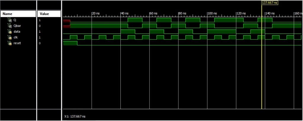
Verilog module of D Flip-Flop. The input to the module is a 1-bit input data line D. The control lines to the module include a 1-bit clock. The output lines are Q and Qbar (complement of output line Q). The output line Q takes the same value as that in the input line D on the rising edge of the clock line Clock when the reset line is at low. Output waveform are shown in figure number 18 below.
Verilog Module for D Flip Flop with set and clear: 
Figure 18: Output waveform of D Flip Flop with reset input
Here in this module we have add two signals named as set and clear. A condition of set=1 give normal operation, while set=0 forces the slave to an output=1. The function of clear input is also same as to the set. When clear=0 the flip flop forces an output to zero, and at clear=1, the output will behave as a normal DFF. One interesting thing here is that clear and set both signals can’t be zero at same time because if set and clear will zero at same time then Q=Qbar, which is not possible. Output waveform and block diagram are showed in figures below.
It is common to find several variations of DFFs in a cell library including features such as input buffers, clock buffers and input with combinational logic gates. One of the type is toggle flip flop or TFF. TFF changes state on every rising clock edge can be created by adding feedback loop Qbar to data input. To establish one at output initially, we have to define an enable/set that perform this job, when set=0 no output will be zero. When set=1 output will be generated, once output generated then TFF follow the inverse of that output. This inverse of TFF’s output is call feedback of3.
Verilog Module for modified DFF to TFF with Feedback:
Block diagram and Output waveforms of TFF are given below.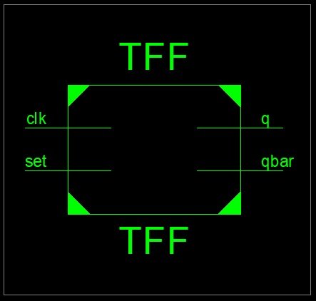

Figure 19: Block Diagram of modified DFF to TFF with Feedback
Verilog Module for CMOS DFF with Load Control:
Figure 20: OUTPUT Waveforms of modified DFF to TFF with Feedback
This is one of the important approach to designing a controlled loading DFF. Here we have to define a signal named as load, which load the data input on pos-edge. After loading there are two ways to hold data at output, when Load = 0, you can observed the output wave forms and complete impact of load signal on output. So at bottom line we are using a control load signal to load and hold the data. At Load=0 output will be hold, as Load =1; output will be update according to new data input. Block diagram and Output waveforms of DFF with Load control are given below.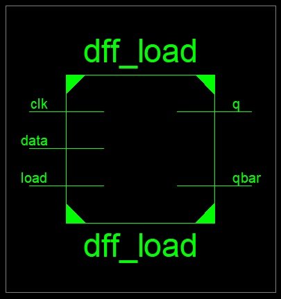
Figure 21: OUTPUT Waveforms of DFF with Load Control Signal
Figure 22: Block Diagram of DFF with Load Control Signal
Design and simulation of D flip flops in Microwind layout designer
Layouts for all these different types of D flip-flops are designed using microwind software. Microwind is basically a tool used for designing and simulation of circuits at layout level. The main advantage of simulating design at layout level is that we can find out errors at layout level and make changes in layout. This tool provides a full facility at layout level. We can see process view and 3D view of design.
We have designed layouts of all these D Flip-Flops and we have used foundry layout of 0025CMOS process. We have tried our best to optimize these layouts as maximum as possible by utilizing minimum area of substrate and where possible by making combining different n+ and p+ regions into common regions. For example, in maximum layouts, NOT gates are used in series and parallel configuration so we combine them into one substrate instead of making two NOT gates separately and similarly in D flip-flops where two MOS are sharing regions with each other we combine these shared regions on single substrate and same we try to optimize these layouts as maximum as possible. Layouts of different types of D Flip-Flops along with their simulation results are shown and explained in section below.
layout of master salve D Flip-Flop with positive edge triggered
layout of master salve D Flip-Flop with positive edge triggered is show below and simulation results. This is a layout of master salve D Flip-Flop with positive edge triggered input D and output Q and its compliment.
Figure: 23 master salve D Flip-Flop
Figure: 24 simulation results of master salve D Flip-Flop
Alternate circuit for mater slave Flip Flop
Alternate circuit for mater slave Flip Flop is show below and simulation results. This is a alternate circuit for mater slave Flip Flop. In this layout, we have used extra NOT gate to give clock and its invert input to different MOFETS in design. Same process is used for other layouts to give clock inputs to layout.
Figure:25 Layout design of Alternate circuit for mater slave Flip Flop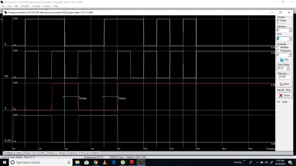
Figure 26: Simulation results of Alternate circuit for mater slave Flip Flop
D Flip Flop with master clear and set
This FF has asserted low clear and set inputs. In this D Flip Flop clear input is used to clear the bit the stored on D Flip Flop and set pin is used to set the data to 1 in FF. So these pins have advantages to set and reset Flip Flip synchronously and asynchronously. It working is already explained earlier section of this paper. Layout and simulation results are shown below.
Figure 27: Layout of example D Flip Flop with master clear and set
Figure 28: Simulation results of example D Flip Flop with master clear and set
D Flip Flop with Feedback
In this design D Flip Flop is modified to T Flip Flop or TFF using Feedback from output to input. So there is no need to input in TFF. Only clock triggered the circuit. Layout of TFF and simulation result verification is show below.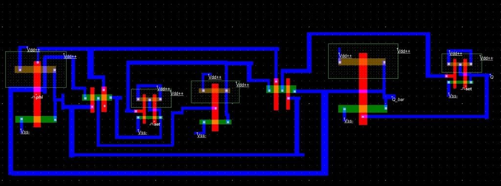
Figure:29 Layout of example D Flip Flop with Feedback
Figure: 30 Simulation results of example D Flip Flop with Feedback
D Flip Flop with Load Control
This is master slave Flip Flop with Load control. When load is zero, No change will happen at the output of Flip Flop and change will only happen load pin is logical high. Layout and simulation verification is shown below.
Figure: 31 Layout of example D Flip Flop with Load Control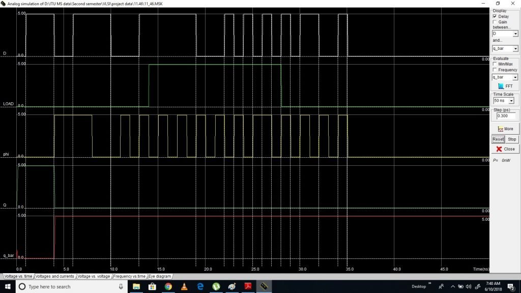
Figure 32: Simulation of example D Flip Flop with Load Control
Conclusion: So in this article, we simulated different types of D flip flops and designed its layouts in microwind software and verify results in Xilinx ISE, DSCH 3 and microwind at layout level.


Can you please share the circuit files so we can change the properties and observe the outputs?
please share the circuit its urgent please