CD4008 4-bit full adder integrated circuit used for binary addition. Binary addition is the base of every function performed in most of the smart machines. It is easy to make a two-bit adder using two simple logic gates. A two-bit adder circuit can be made just by using XOR and AND gate. It comes up with two inputs and two outputs. The two bits are only applicable to add two bits, to make full adder we can use two half adders but after simplifies the combination of half adder circuit a full adder circuit was designed.

Full Adder is made of one OR, two XOR and one AND gate. It has three inputs and two outputs. The First two inputs use as two input data bits and the third input is used as carrying bit, which we have no further use in half adder circuit. The output carries a bit on full adder circuit transfer the carry bit to the next adder and it performs the addition by considering three input values.
Introduction to CD4008 4-Bit Full ADDER CIRCUIT
The multiple full adders could be used as a multiple bit adder circuits. CD4008 IC is a full 4-bit adder circuit which comes up with a combination for four full bit adders. It could add four multiple bits without any error. It carries a bit from state to stage and perform the addition. CD4008 is one the fastest and high voltage adder circuit with carrying out feature.
Pinout of CD4008
The pin configuration and details of all input outputs pins are listed below:

PIN CONFIGURATION CD4008 4-Bit Full ADDER
| PINS | DETAILS | |
|---|---|---|
| A4 | Pin 1 | Pin 1 will be used by the first bit of 4-bits input data A of full adder. It could either be 1 or 0. |
| B3 | Pin 2 | Pin 2 will be used by the 2nd bit of 4-bits input data B. |
| A3 | Pin 3 | Pin 3 will be used by the 2nd bit of 4-bits input data. |
| B2 | Pin 4 | The third bit of 4-bits input data B will be given as input on Pin 4. |
| A2 | Pin 5 | The third bit of 4-bits input data A will be given as input on Pin 5. |
| B1 | Pin 6 | The last bit of 4-bit data B will be input at pin 6. |
| A1 | Pin 7 | The last bit of 4-bit input data A will be input at Pin 7. |
| VSS | Pin 8 | CD4008 is a logic-based device. It will be required power to turn on or we can say to it will require Ground to operate with other devices. VSS pin will be used as Common Ground. |
| C1 | Pin 9 | C1 will be the carry input bit of the first adder in IC, which will be given on pin 9. |
| S1 | Pin 10 | The last bit of the added value will be out at Pin 10. |
| S2 | Pin 11 | Pin 11 will represent the 3rd output bit of the added value. |
| S3 | Pin 12 | Pin 12 will be used for 2nd output bit. |
| S4 | Pin 13 | First output bit will be received at Pin 13. |
| CO | Pin 14 | Last carryout bit will be at Pin 14. |
| B4 | Pin 15 | Pin 15 will be used by the first bit of 4-bit input data B |
| VDD | Pin 16 | VDD will be used as power input. |
FEATURES of CD4008 4-Bit Full ADDER IC
- 4-bit full adder with carrying out features
- Parallel input and output method
- High operating speed without any interruptions
- Available with 16-pins in PDIP, CDIP, SOIC, and TSSOP Package
- Meets all the requirements of all CMOS devices.
- It has HIGH operating voltage as compared to most of the other CMOS devices.
SPECIFICATIONS of CD4008
- The total time required for values from input to output is 160ns.
- It has a noise margin at different voltages:
- 5V margin will be about 1V.
- 10-volt margin will be about 2V.
- 15 Volt margins will be about 2.5V
- CD4008 normal operating voltage rages are 5- 15V, it could operate also maximum at 20V
- Maximum input current should be 1uA at 18V.
- The temperature should be 25 degrees at 18V and 1uA
- Most of the specifications and features only work when IC is operation at exact 5V.
WORKING of CD4008 4-Bit Full ADDER
As we discussed early CD4008 is a combination of 4 full adder circuit. So First we need to understand how single full adder works. A full adder circuit works with logic gates. It has a combination of two XOR, two AND gates and one OR gates. Here is the following internal circuit of Full Adder.
In above circuit diagram, the First XOR gate will be used as adding the two inputs and then the second XOR gate will be used for sum up the output from first XOR and Carry in. The other two AND gates and OR gate will use to find out the carry out from the input values and from previous carry in. The output will give us two values one is the output of input values and the other one is carried of the input values. If we gave only one input value then there will be output, there is no case in which there will be no output. The output for CD4008 full adder will follow the following truth table pattern.
Full ADDER Table
| TRUTH TABLE | ||||
|---|---|---|---|---|
| Cin | Input (A) | Input (B) | Sum (S) | Cout |
| 0 | 0 | 0 | 0 | 0 |
| 0 | 0 | 1 | 1 | 0 |
| 0 | 1 | 0 | 1 | 0 |
| 0 | 1 | 1 | 0 | 1 |
| 1 | 0 | 0 | 1 | 0 |
| 1 | 0 | 1 | 0 | 1 |
| 1 | 1 | 0 | 0 | 1 |
| 1 | 1 | 1 | 1 | 1 |
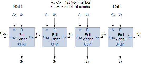
In CD4008 the single adder will follow the above truth table on specific inputs. The internal structure of CD4008 will be the combination of four full adders. Expect the first adder, each will take two inputs from the user or from another device and the third input will use the carry-out value of the previous adder. The first adder will receive the first carryout input from outside the IC and the last carry out of the last adder will be used as an output value. This combination of 4 adders will work in series.
The 4-bit full adder circuit starts adding from the least significant bit (LSB) and keep it doing till the most significant bit (MSB). It has the ability to solve the carryout problem. Most people think that two half adders could make a full adder which is true but two half adders could be used as full adder but their structure will be more complex as compared to the single full adder. The full adder is the simplifies version of the combination of two full adders.
APPLICATIONS of CD4008 4-Bit Full ADDER
- It is used for High-Speed Arithmetic Operations.
- CD4008 also used as miniature calculators.
- Counters also have some use of CD4008.
- It is also used in Simple Logic Design
EXAMPLE in Proteus
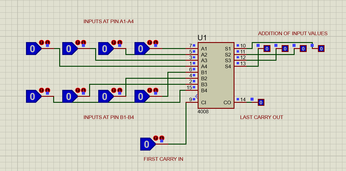
Now, we will see simple binary addition example in proteus. Here we will use CD4008 for the addition of four-bit data. First, add CD4008 in proteus, then attach the logic state viewer and logic state provider to CD4008. Attach the logic states as shown in the circuit. The last bit of both input values should be at A1 and B1 because addition always starts from the last digits.
After making the circuit as shown in proteus, start to send the desired values. First, let’s do an addition on specific 4-bit digits mathematically. Suppose: A = (1010)2 , B = (1000)2 ,Carry in = (1)2. When we add all these three values we get the output (10011) 2.
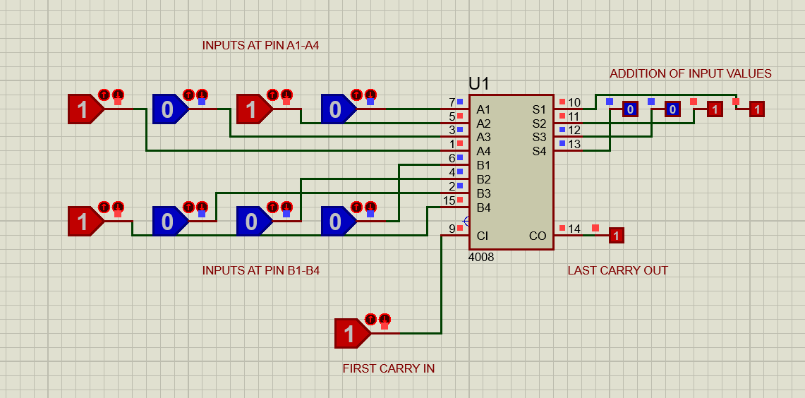
Now here let’s try the same at CD4008.
Here in the output of proteus, you may notice that we have “0011” at the output, which is the same as the last four bits of our mathematical output. In proteus we have only four bits is because it’s a four bit full adder circuit and its output will be four-bit the remain will be considered as carrying. The MSB of our mathematical output is “1” which is equal to the carryout in Proteus.
How to Convert 4-bit to 8-bit or More?
The CD4008 can expand to an 8-bit adder by attaching two ICs or it could go further. The only thing we need to make sure about the input values on the pin. If input values get shuffle then it becomes impossible to get the correct output. The correct output will always be dependent on the input value. During using CD4008 always verify the input pins and their values to avoid any mathematical error.
Proteus Simulation
You may also like to read: