TLP250 is an isolated IGBT/Mosfet driver IC. The input side consists of a GaAlAs light-emitting diode. The output side gets a drive signal through an integrated photodetector. Therefore, the main feature is electrical isolation between low and high power circuits. It transfers electrical signals optically via light.
Users can use it to drive gate terminal of high voltage switches in both configurations such as high side and low side drive. It is available as an 8-pin DIP package.
We have already posted an article on non-isolated gate driver IR2110. MOSFET driver IR2110 is used to drive n-channel or p-channel MOSFETs in the high side and low side.
What is a MOSFET/IGBT driver?
It is the main component of power electronics circuits. Mosfet driver is dedicated to integrated circuits that are used to drive gate terminal of power switches both in the low side and high side configuration. To know more about gate driver check the following article:
Pinout diagram TLP250
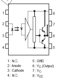
The Pinout diagram of TLP250 is given below. It is clearly shown in the figure that led at the input stage and photodetector diode at the output stage is used to provide isolation between high and low power circuits.
Pin number 1 and 4 are not connected to any point. They are marked as NC ( No connection). Hence they are not in use. Pin 2 is the anode point of input stage light emitting diode and pin 3 is the cathode point of the input stage. Input is provided to pin number 2 and 3. Pin number 8 is for supply connection. Pin number 5 is for a ground of power supply.
Pin Configuration Description
Details are according to the datasheet.
| PINS | Details |
|---|---|
| 1. NC | .No Connection – Not used |
| 2. Anode | Anode terminal of LED diode |
| 3. Cathode | The cathode terminal of LED |
| 4. NC | .No Connection – Not used |
| 5. GND | Connect with Ground of power supply |
| 6. Vo | Output terminal |
| 7. Vo | Output terminal |
| 8. Vcc | Connect with Positive terminal of power supply |
Pins Functions
- Pin number one and four is not connected to any point physically. Therefore they are not in use.
- Pin number 8 is used to provide power supply to TLP250 and pin number 5 is a ground pin that provides a return path to power supply ground. A maximum power supply voltage between 15-30 volt dc can be given to TLP250. But it also depends on the temperature of the environment where it is being used.
- Pin number 2 and 3 are anode and cathode points of input stage LED. It works like a normal light-emitting diode. It has similar characteristics of forwarding voltage and inputs current. The maximum input current is in the range of 7-10mA and the forward voltage drop is about 0.8 volt. TLP250 provides output from low to high with a minimum threshold current of 1.2mA and above.
- Pin number six and seven is internally connected to each other. Output can be taken from either pin number 6 and 7. Totem pole configuration of two transistors is used in TLP250. In case of high input, the output becomes high with output voltage equal to a supply voltage and in case of low input, the output becomes low with output voltage level equal to ground.
- Mosfet driver TLP250 can be used up to 25khz frequency due to slow propagation delay.
This all about pin configuration and now we will see how it works.
Isolated MOSFET driver working
TLP250 has an input stage and an output stage. It also has a power supply configuration. It is more suitable for MOSFET and IGBT. The main difference between this and other MOSFET drivers is that it is optically isolated. Its mean input and output side are isolated from each other electrically. But electrical signal transfers between both sides through an optical signal. It works like an optocoupler. The input stage has a light-emitting diode and the output stage have a photodiode. Whenever the input stage LED light falls on the output stage photo detector diode, the output becomes high.
Now we will talk about how to used isolated IGBT drivers as low side gate driver and high side gate driver.
Electrical Features and Specification
- Operating frequency: 0-25kHz
- Input Supply voltage: 10-35 volts
- Output voltage: 10-35 volts
- Output drive current: 1.5A
- Electrical isolation voltage: 3500 VRMS
- Switching rise and fall time: 1.5μs
- Operating temperature range: -20 – 85 degrees
TLP250 IGBT Driver Examples
Low Side Gate Drive Example
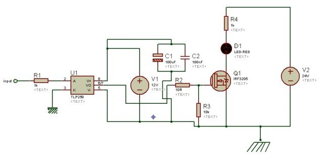
Circuit diagram of low side Mosfet driver using tlp250 is shown below. In this circuit diagram, tlp250 is used as a non-inverting low side Mosfet driver. you should connect an electrolytic capacitor of value 0.47uf between the power supply. It provides protection to tlp250 by providing stabilize voltage to IC.
As shown in the figure above input is a drive signal that drives the output. Vin is according to signal ground. It should not be connected with the supply ground and output ground. It is clearly shown in the above figure TLP250 and load ground is referenced to the power ground and it is isolated from input signal reference ground. When an input is high, MOSFET Q1 gets a high signal from TLP250 and it is driven by a power supply and current flows through the load.
When an input is low, MOSFET Q1 gets a low signal from a TLP250 output pin and Mosfet Q1 remains off and there is no current flow to load. The value of supply voltage ranges between 10-15 volt. The input resistor at the gate of MOSFET is used depend on the amplitude of the input signal. Usually, the input signal is provided through microcontroller and the microcontroller input signal level is in the order of 5 volts. Capacitor C1 is used as a decoupling capacitor.
TLP250 as a high side MOSFET/IGBT driver Example
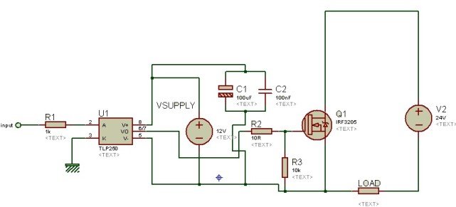
Circuit diagram of MOSFET/IGBT driver tlp250 used as high side driver is shown below. It is used as a non-inverting high side gate drive circuit. Because input signal ground is connected to the cathode of the input stage light emitting diode. Therefore it is used as a non-inverting high side gate driver.
In high side configuration, there are three grounds as shown in the figure above. The ground of input signal, a ground of supply voltage and ground of power supply voltage. Remember that while using TLP250 as high side MOSFET driver, all grounds should be isolated from each other.
TLP250 Applications
- Induction heating
- Solar heating system
- Solar inverters/ Power Inverter
- Pure sine wave and modified sine wave inverters


Hello. Thank you for posting.
I have a question. How could I select the value of R2 and R3?
And in datasheet, they recommend to connect 0.1uF bypass capacitor between pin 8 and pin 5, but in your figure, C1 and C2 values are 100uF and 100nF respectively. which one is suggested?
And one more question. How could I isolate the ground of supply voltage and power supply as High side mosfet driver. In figure, they are all connected in same point.
just use them separately
it doesn’t matter in most applications
Sir, how do I provide 20kHz frequency to trigger a mosfet with this driver?
Both 100ufd and 100nf are desirable. The larger provides a low impedance power supply source, and the smaller is better for bypassing high frequency noise or spikes. Because neither is an ideal capacitor due to internal construction characteristics the electrolytic and polyester or ceramic do different jobs.
Is it possible to switch a 220v dc supply to load using tlp250
sir what value of capacitors should be used to make proper operation of ir2104 driver..
thans in anticipation.
I have a problem of using tlp 250 is that i am not getting output from pin number 6…i have given pulse to pin num 2 through the Arduino…. nd at pin num 8 12 volt dc vol…
Hello sir I have also the same problem but i have given pulse to pin 2 through 555 timer plz reply if u get output from tlp250 at pin 6
why tlp 250 gets damaged easily?
Hey All I have 1 question.
Can I use ULN2003A instead of TLP250?
How can i add TLP 250 optocoupler to protoeus Isis to make a pcb ?? i need help plz
i will be tnankfull
utilice el HCPL-3120
sir can we give constant dc supply to 2nd pin of tlp250 ic…
Salam how can we calculate the value of resisters, capacitors
What is the maximum bus voltage of TLP250?
One question sir I want to design circuit for (3 phase induction motor operating voltage 42vac 80w)control by MOSFET..
But I have no idea to design so, pl help.
Thanks u
Warm regards
Vinay Kumar
vinay00779@gmail.com
Apakah TLP 250 sama dengan AT250V
hi
can i connent supply range 20 volte to them?tl250
hi i cant find tlp250 library to use
can you help me or send me ?
sir, your R2 resistance is how much ohm?
10 ohm or 10kohm?