LM201 is a general-purpose amplifier that can be used as an advanced alternative of LM741 OP-AMP with an extensive overload protection on the input and the output. It is available in the market as plastic package N DIP 8 and plastic micro package DSO 8. The best advantage it has over internally compensated amplifiers is that the compensation is adjusted in accordance with a particular application. The corresponding family members of LM201 are LM101 and LM301 which differ each other in certain specifications. The slew rate of 10V/µs and bandwidths of 3.5MHz can be obtained with much ease.
LM201 Pinout details
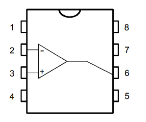
LM201 comes as 8 PIN IC with basic pins for applying inverting and non-inverting inputs and for obtaining the output. DC supply voltage Vcc can vary from ±5 to ±22 Volts.

| PINS | Details |
|---|---|
| 1 – ( Balancing Compensation 1) | This pin is for compensation |
| 2 – ( Inverting Input) | This pin for applying the inverting input voltage |
| 3 – (Non-Inverting Input) | This pin is for applying a non-inverting input voltage |
| 4 – (-Vcc) | This pin is for applying negative DC supply |
| 5 – (Balance) | This pin is for balancing |
| 6 – (Output) | This pin is for obtaining an output voltage |
| 7 – (+Vcc) | This pin is for applying positive DC supply |
| 8 – (Compensation 2) | This pin is for compensation |
LM201 Features
- Input offset voltage : 0.7mV
- Input bias current: 25nA
- Input offset current: 1.5nA
- Slew rate as inverting amplifier: 10V/µs
- Supply voltage rejection ratio: 96dB
- Large signal voltage gain: 100 V/mV
- Supply no load current: 1.8mA
- Common mode rejection ratio: 96dB
- Output short circuit current: 30mA
- Maximum output voltage swing: 14V
- Input impedance: 4MΩ
You may want to download a datasheet of LM201 to read further on the electrical specifications of a single-channel op-amp.
Where and How to Use LM201
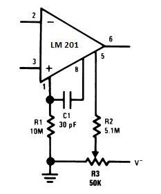
LM201 IC is specially designed to protect when overloaded on input and output. It bypasses the struggle of oscillations and compensations by a simply 30pF capacitor. Higher bandwidth makes it possible to use it as a versatile amplification device. While using LM201 input signal is either applied at inverting or non-inverting input terminals i.e. pin no. 2 or 3. DC supply voltage ranging from 5-22V is applied on pin no. 4 & 7 in such a way that the negative potential of the battery is connected to pin 4 while positive to pin 7. The output voltage is obtained at pin 6. Pin 1, 5 and 8 are used for balancing and compensations. Specific configurations are available to do standard compensation and offset balancing.
LM201 Example 1
One such configuration is shown as:
More Example Ideas
LM201 can be used for the construction of:
- fast summing amplifier
- fast voltage follower
- bilateral current source
- fast AC/DC converter
- instrumentation amplifier
- voltage comparator for driving RTL logic or high current driver
- low frequency square wave generator
- voltage comparator for driving DTL or TTL Integrated circuits
- isolating large capacitive load
- sine wave oscillator
- fast half wave rectifier
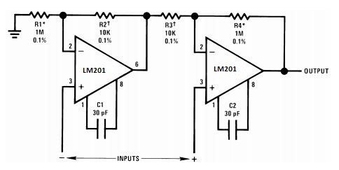
precision amplification using LM201
One of the common use of OP-AMP is precision amplification or instrumentation amplification. The cascaded form using two LM 201 Op AMPs is shown below where R1=R4 and R2=R3 with Av = 1+ (R1/R2).
You can check these practical guides where we used operational amplifier for AC voltage and AC current measurement.
- AC Voltage measurement using PIC16F877A microcontroller
- alternating current measurement using pic microcontroller
LM201 Applications
The real-life applications of LM201 are:
- on our mobile phones for AD conversion
- In Audio amplifiers
- Video signal conditioning units
- Sensor Data Accusation
- weighing scale (electronic)
- digital to analog converters in Phone
- Temperature control in various device
- error amplifiers
- communication circuits
- Receivers
- Modulators
- Synthesizers
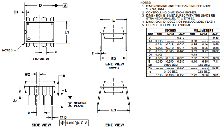
2D Model Diagram
We always need a 2D model of an integrated circuit while designing a printed circuit board. This figure represents the 2D model dimension for the DIP package. You can consult the datasheet for 2D model of other packages.