74LS323 is an 8-bit universal shift-storage register having 3-state outputs with the feature of Synchronous Reset. Pin count has been minimized in it using parallel load inputs and flip flops outputs. In order to provide cascading without any trouble, separate inputs and outputs are available for flip-flops.
74LS323 Pinout
Following figure shows the pinout diagram of 74LS323 IC.

Pin Configuration Details
The detailed description of all pins of SN54/74LS323 is given below.
- CP (Clock Pulse) : This is an input pin and fed with a clock pulse. It is an active positive rising edge pin.
- DS0 (Right shift serial data input ) : This data pin is used to feed data on which function of right shift will be performed. It is a serial data input pin.
- DS7 (Right shift serial data input ) : This data pin is used to feed data on which function of left shift will be performed. It is a serial data input pin.
- I/O1 to I/O7 : These are 8 input and output pins. These are used to handle parallel data input and outputs.
- ~OE1, ~OE2 : These pins are used to enable output function of I/O pins. These are active low input pins.
- Q0, Q7 : These are serial output pins and are used to cascade the ICs.
- S0, S1 : These are input pins to select mode of IC.
- ~SR : This pin is used to perform the function of synchronous reset. This pin is an active low input pin.
- VCC and GND : These pins are used to power up the IC.
SN54/74LS323 Modes of Operation
This shift register IC has the ability to perform the following four functions.
- Left Shift
- Right Shift
- Hold (Store)
- Parallel Load
Internal Logic Diagram
The internal logic diagram of 74LS232 shift register IC is shown in the figure below. It consists of a number of AND, OR, NAND, NOT gates, and 8 edge-triggered D type Flip-Flops. These flip-flops make transitions of data on the positive edge of the clock only.

Truth Table for working of 74LS323 is shown in the figure below. It shows the relation of input pins and their response on output pins.

74LS323 Working
Following is the working of this particular IC.
Synchronous Reset
~SR is an active low input. So until its state is low none of the above mentioned four operations left, right shift, hold and parallel load can be performed. In order to perform any function, it should be in high state.
Select Mode of Operation
S0 and S1 are used to select mode of operation. Following is the coding of the inputs.
- When S0 = S1 = High. Parallel Load operation is performed.
- When S0 = S1 = Low. Hold Operation is performed.
- When S0 = High and S1 = Low. Right Shift operation of Data at DS0 takes place.
- When S0 = Low and S1 = High. Left Shift operation of Data at DS7 takes place
Enable Output
~OE1 and ~OE2 are output enabled pins. Following is the coding of these inputs.
- When ~OE1 = ~OE2 = High. Status of I/O pins is undetermined.
- When ~OE1 = High and ~OE2 = Low. Status of I/O pins is undetermined.
- When ~OE1 = Low and ~OE2 = High. Status of I/O pins is undetermined.
- When ~OE1 = ~OE2 = Low. Status of I/O pin can be determined and depends upon available data in IC.
CP is a clock pulse input pin and all operations are performed at the positive edge of the clock pulse. DS0 and DS7 are the serial input data on which operations will be performed.
74LS323 Shift Register Proteus Software
Function of different pins can be confirmed through simulation in Proteus software.
1. Below figure shows that until both ~OE1 and ~OE2 are high. Status of the IO pin is undetermined.

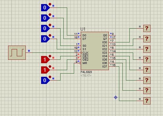

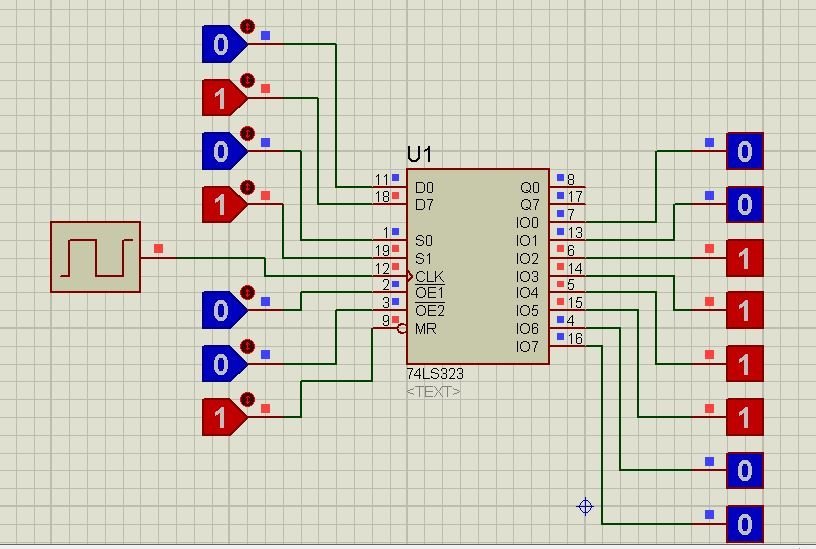
2. Below Figure shows until MR (~SR) is low, IO pins status is low no matter what is being fed at as serial data input at D0 (DS0) and D7(DS7).


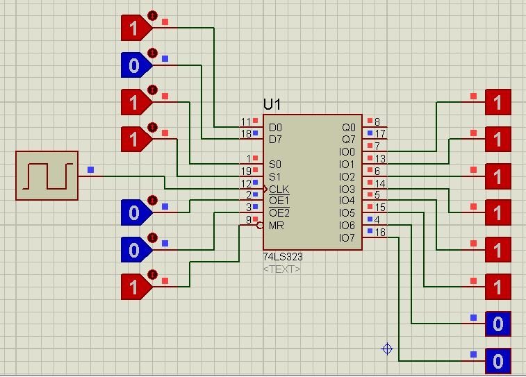
3. When both S0 = S1 = low. Hold operation takes place and whatever data is at output. It stops there and holds the output states of pins.

4. Suppose that data was hold as in above figure. Now if we set S0 = high and S1 = low. Right shift operation of data at input D0 (DS0) takes place.

5. Suppose that data was hold as in below figure.

6. Now if we set S0 = low and S1 = high. Left shift operation of data at input D7 (DS7) takes place.
7. When S0 = S1 = High, parallel transfer operation takes place. Means whatever is at Q0 to Q7 pins inside IC is transferred at IO0 to IO7 output pin respectively. As only Q0 and Q7 is provided at output so it can be verified in the following manner that at this state IO0 = Q0 and IO7 = Q7 will appear at output pins.
74LS323 Series Ordering Code
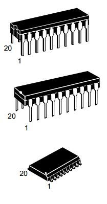
This IC comes in with three variants as shown in figure below.
Ordering format for these are as follows.
- SN54LSXXXJ
- SN74LSXXXN
- SN74LSXXXDW
XXX=323 and J represent that it is made up of ceramic. N represents it comes in plastic casing and DW is SOIC packaging.
Features
Following are the distinguished features of this IC
- Common I/O pins which reduce the pin count and space occupied by IC
- Feature of synchronous reset which other ICs that perform shift function don’t have.
- 3 state output and this feature can be used for bus oriented applications.
- Clamp diodes at input which limit the effect of high speed termination.
- Separate continuous inputs and outputs from pin Q0 and Q7 which gives the ability to be cascading one IC with other IC.
- Capability to handle electrostatic discharge with more than 3500 V.
- Perform four operations i.e. left shift, right shift, parallel load and hold function of data.
Applications
Following are the few applications of this IC.
- It can be used in a sequence generator.
- This has find its application in control circuits and code conversions.
- This IC is used for counters and Arithmetic unit registers.
- This IC is used for serial to parallel and parallel to serial data conversion.
Related shift register ICs and their used in projects:
- 74LS164
- 74LS166
- 74HC595 Serial Shift Register Interfacing with Pic Microcontroller
- CD4015
- 74HC595 Shift Register
- CD4035 4-Stage Parallel in Parallel out Shift Register
- CD4014
- Expand Output Ports of Arduino by Using IC74HC595N
- Shift registers in LabVIEW examples
- 74HC595 Interfacing with 7-segment Display and Pic Microcontroller
- MAX7219 Interfacing with 8-digit 7 Segment Display and PIC16F877A