Before starting with 74LS73 DUAL JK FLIP-FLOP, let’s first understand that what is it? Flip-Flops and latches are those small devices used to store a single bit. A single flip-flop represents two-state, in which data is stored is represented by 1 and the other is represented by 0. An SR latch has two problems. In SR latch the S = R = 0 should be avoided by the system. The other problem is the correct latching problem may not occur when the enable pin is high. To solve this problem a JK flip flop is used. JK flip-flop comes up with an internal SR latch circuit, but it also has a clock installed. The clock solves these two problems. JK flip flop was named by the designer name Jack Kilby. JK flip flop clock gives some extra functions too. It gives four input combinations, which are logic 1, logic 0, no change and the third one is a toggle.
Introduction to 74LS73 DUAL JK FLIP-FLOP
Now comes the 74S73 DUAL JK FLIP FLOP, whenever we need two JK flip flop at the same time then 74S73 DUAL JK FLIP FLOP IC is the best option. It has an internal two JK flip flop. Both have a different structure. They both do not even depend on each other or anything. The user could even use a single flip flop without using the other.
Pinout of 74LS73 DUAL JK FLIP-FLOP

PIN CONFIGURATION of 74LS73
| PINS | DESCRIPTION | |
|---|---|---|
| 1 CLK | Pin 1 | Pin 1 is the clock pin for first JK flip-flop. Change of pulse is used to change the state. |
| 1CLR (BAR) | Pin 2 | Pin 2 used as resent pin for first flip-flop. LOW pulse will be used to clear the data from the flip flop. |
| INPUT K-1 | Pin 3 | K-1 is the input pin used to send the bit to the JK flip flop. |
| VCC | Pin 4 | Vcc is used to apply the power supply to the JK flip flop to the whole IC. |
| 2CLK | Pin 5 | Pin 5 is used to provide the clock to the second JK flip flop in 74LS73. Change of pulse from LOW to HIGH used to change the state. |
| 2CLR (bar) | Pin 6 | Pin 6 is used as a reset pin by second JK flip-flop. LOW pulse will be used to reset the data from the flip flop. |
| INPUT J-2 | Pin 7 | It is used to send the second input of JK flip flop. |
| OUTPUT 2Q (bar) | Pin 8 | Pin 8 is used as an inverted output of second JK flip flop. |
| OUTPUT 2Q | Pin 9 | Pin 9 is used as the non-inverted output of the second JK flip flop. |
| INPUT K-2 | Pin 10 | Pin 10 is used as an input pin for second JK flip flop. |
| GROUND | Pin 11 | The ground pin is used to apply the ground of power supply and to make the common ground of another circuit with IC. |
| OUTPUT 1Q | Pin 12 | Pin 12 gives the non-inverted output from first JK flip flop. |
| OUTPUT 1Q (bar) | Pin 13 | Pin 13 gives the inverted output from the first JK flip flop. |
| INPUT J-1 | Pin 14 | Pin 14 used as a second input for first JK flip flop. |
FEATURES 74LS73 DUAL JK FLIP-FLOP
- It operates for all kind of TTL/EMOS devices.
- It could store a single bit like other latches but it has the ability to give the toggle and no change state.
- 74LS73 could store two bits at the same time.
- It doesn’t have any error state and invalid state like some other latches.
- Its operating temperature range is 0 – 70 degree and the charge storage temperature range is -65 to 150 degrees.
- 74LS73 comes with two types of packing, SOIC, and PDIP.
WORKING of DUAL JK FLIP-FLOP

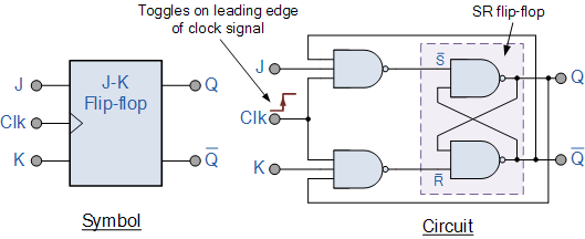
To understand 74LS73 we need to understand SR latch first. In SR latch there are two inputs. First, one is Reset and the Second one is known as a set. The output should be HIGH at least one pin and another pin should be at a LOW state. There are four logic states in which SR latch operates, which is when there is different input on both input pins but when there are same outputs then in case of 1,1 the output becomes invalid and in case of 1,1 the output becomes unpredictable. So, to solve this issue in JK flip-flop an internal clock has been installed. The clock controls the change in output with the input state.
JK flip flop comes up with two SR latch and four NAND gates as you can see in the below image. The first latch is used as Master and another SR latch is used as Slave. The two NAND gates and Slave SR latch gives the input to Master SR Latch. The output of the Slave latch to Master helps the JK flip flop to toggle. pulse. The input signal of Master is connected to the NAND Gates. The output of the NAND gates has been attached to anther pin which is known as clock pin. Clock pin only allows the NAND gate
to give the output to the master when the CLOCK get a rising pulse. When the clock is LOW then there will be no output. The output will be ignored in case of LOW Pulse. The output of Master Latch will be given to the Slave when there will be HIGH to LOW pulse to the Input gate of Slave Latch. This clocking process between Master and Slave makes the flip flop to transfer the data from the master to slave with a timing signal.
Table of Dual JK Flip Flop
The following outputs will be done on given inputs.
| TRUTH TABLE FOR JK FLIP FLOP | |||||
|---|---|---|---|---|---|
| CLOCK PULSE | INPUTS | OUTPUTS | DETAIL | ||
| CLK | J | K | Q | Q’ | |
| X | 0 | 0 | 1 | 0 | NO CHANGE |
| X | 0 | 0 | 0 | 1 | |
| L – H | 0 | 1 | 1 | 0 | Same as SR Latch |
| X | 0 | 1 | 0 | 1 | |
| L – H | 1 | 0 | 0 | 1 | |
| X | 1 | 0 | 1 | 0 | |
| L – H | 1 | 1 | 0 | 1 | Toggle Action |
| L – H | 1 | 1 | 1 | 0 |
L-H = low to High Pulse
X = No change of Pulse
APPLICATION of 74LS73 DUAL JK FLIP-FLOP
- It is used as shift registers.
- The latching and EEPROM circuit uses the JK Flip Flop.
- JK Flip Flop has wide use in RAM.
- Due to its fast speed, it was widely used to control the specific LED Pattern.
- JK Flip Flop used as Memory and Control Registers.
Datasheet 74LS73 DUAL JK FLIP-FLOP
Example with Proteus
In Proteus first, understand how Flip Flop will work. When we give the logic one state on the J and zero on K then we receive the one on the Q and zero on Q’, and when we send the zero on J and one on K then we receive the one Q’ and zero on Q. This whole process will follow the truth table as we mentioned above. The clock pulse is continuously changing with time to change the output.
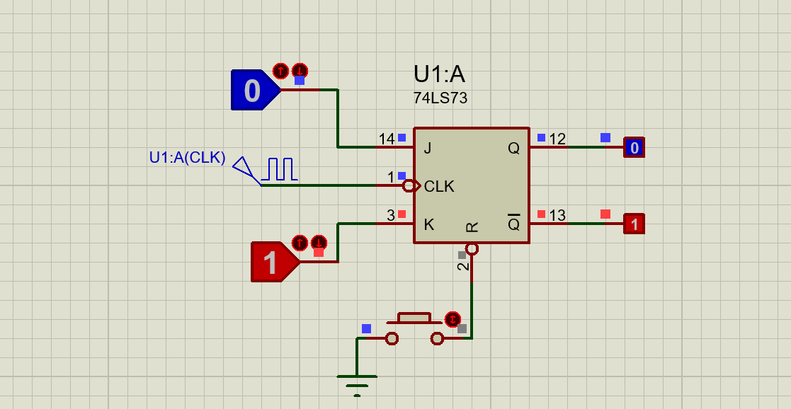
Now here we will understand the other two states. Now Apply the HIGH logic at the “J” then you may notice that Q is turned one, but when you even tried to change the logic at “J”, it will not be affected. Because this shows that a bit has been stored in flip flop. To remove the stored bit just use the reset button. In digital devices, this reset function could be done digitally. The reset button will clear the bit from all the output pins but If we use another method like turn “J” to LOW and “K” to HIGH then bit will shift from Q to Q’. This shifting isn’t from Q to Q’. It comes from the K.
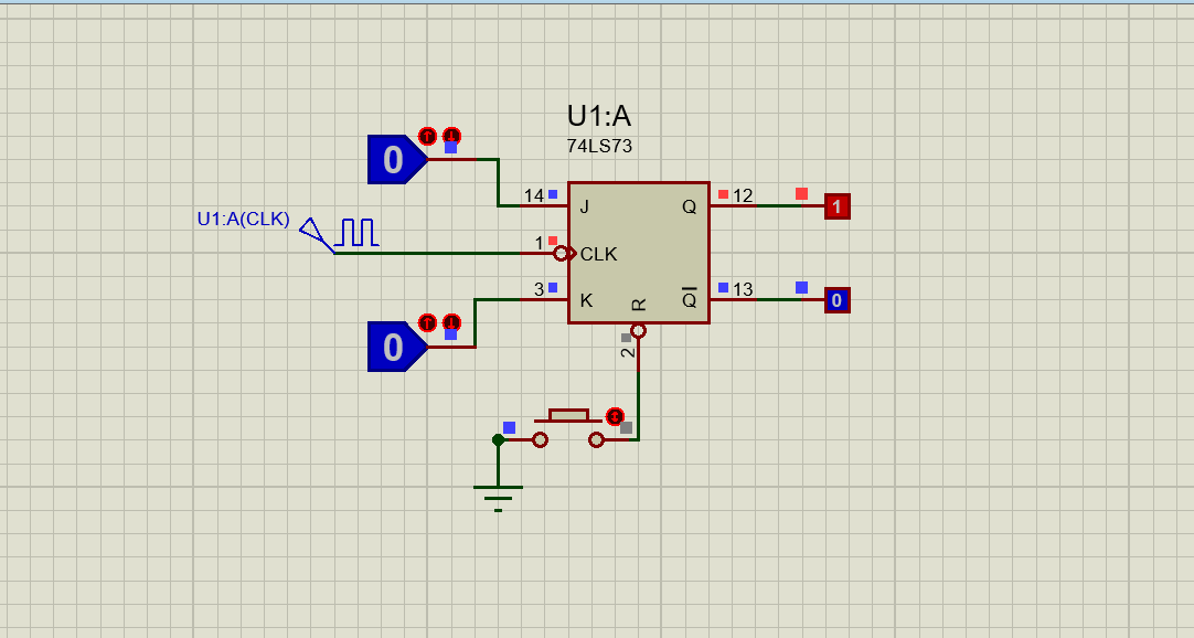
Now we will discuss the last state which is one on both inputs. When we apply the one on both inputs than one on output will toggle. The output will not be stable. It will keep changing with the speed to the input clock signal. These all four effects describe how to flip flop will store the data and will avoid sending the invalid data from the flip flop.
I Can’t design Flip-Flop logic diagram by using three input NAND Gates and two input NAND Gates combined together, There are gray indicators on the logic output. Pls. advice.
Best regards,
Parkesit Danial