ADC0804 is an 8-bit analog to digital converter IC which can measure up to 8 analog input simultaneously. That means the digital output value can vary between 0 to 255. It uses a successive approximation converter which is based on the differential potentiometric ladder.
Every device cannot perform each and every operation. There are always different devices that can perform the different operations and convert them for other devices to perform another’s function. The basic problem we face is the translation of data between these devices.
In Electronics Most of the time, different methods of communication between different devices were invented so different devices could perform efficiently with two or multiple different objects and devices.
Why Do We Need to Use ADC?
When it comes to real-life or we can say in the time domain the output of different events can always represent in mathematical form or mathematical values. These mathematics values are always in continuous form. In other words, we can say these values always have starting and ending point but between these two points, they have infinite values.
These analog values are easy to read in the time domain (real life). When it comes to machines or electronic devices most of them are unable to read them properly. They could read their starting or may ending point but most of the cases they are unable to read them properly. Machines and Electronic devices always perform their operations in the “frequency domain”. To solve this kind of issues we usually use Analog to Digital Converters (ADC).
ADC0804 Introduction
There are multiple kinds of Analog to Digital Converters (ADC) which are used to convert the analog signal for microprocessors or controllers. Every “ADC” has its own specification and advantages on the basis of the requirement. Here we are going to discuss “ADC0804 IC” which is known as the low voltage 8-bit analog to Digital Converter.
ADC0804 is a low voltage IC use to convert the low voltage analog signal to an 8-bit digital signal. It works with 0-5 Volts, has 1 Analog input and 8 output pins. ADC0804 comes with an internal clock but to increase or change the clock cycle we could use the external clock. Always keep in mind that conversion speed cannot be faster than 110us either we are using an internal clock or external clock.
Internal Circuit
Like other electronic devices ADC0804 also has a little complex internal circuit. ADC0804 translates the analog signal to Digital but to convert the analog signal it uses Gates, Flipflops, Shift Register, Tristate, Clock, latch and Ladder and Decoder, etc. But the main components used in ADC0804 to convert the signal is SAR Latch.
SAR Latch converts continuous analog signal to digital signal/discrete signal through a binary search by using all possible quantization/mapping levels. Other components in “ADC0804” like tri-state, 8-bit shifter, etc are used to give the proper output according to the given input. Tri-state is an internal register that is used to hold the data until a high to low pulse is given. An 8-bit shift register is used to give the output in a sequence so other devices could read in the form of 8-bits.
ADC0804 ADC Pinout
The followin picture shows the pinout diagram of ADC0804. It consists of 20 pins.

Pin Configuration
- CS: It stands for Chip select. CS Pin is used to turning on the device. When we are using multiple ADC then this pin is used to select the required device at that time. It’s active at a low state.
- RD: It stands for reading. Its an input pin. RD pin is used when we want to receive the output value from the internal register. High to Low pulse will be used to perform the operation.
- WR: It stands for Write. WR is an input pin used to start the conversion by applying high to low pulse
- CLK IN: It is an input pin used to which represent clock. To apply the external clock this pin will be used.
- INTR: It is an interrupt pin used to indicate that conversion is complete. It goes low when the conversion is completed.
- Vin (+): It is an analogue input pin used for the non-inverting signal. Mostly devices give the analogue signal in the non-inverting form so we use this pin as analogue input.
- Vin (-): It is an analogue input pin used for inverting signals. Due to Signal nature mostly in non-inverting form, this pin attaches to the ground.
- AGND: This pin is used for the ground of Device where analogue input came from.
- View: It is used for giving the voltage reference to current full-scale reading.
- DGND: This pin is attached to the ground of the device where the digital output goes to.
- DB0 – DB7: These pins are used for digital output in 8-bit form.
- CLK R: This pin is used for RC timing to use the internal clock.
- VCC: It is used for providing the power to the whole IC. It should not be greater than +6.5 Volts. Mostly +5.0 Volts are used.
ADC0804 Features
- It is compatible with all microcontrollers and microprocessors which operate at 5 Volts.
- It could calculate different voltages from 0 to 5 by using only a single 5 volts supply.
- Works with different voltage references. The minimum should be 2.5 V.
- Fully functional with CMOS and TTL electronics devices.
- It has an internal clock with frequency 640KHz.
- It works without zero adjustment
- Minimum conversion time is 110us
- Consist of usual 0.3-inch width with 20-Pin DIP Package
- Consist of Differential analog voltage input.
- Digital out range is from 0 – 255
- Input voltage range 2.5 – 6.5
- Operate as a standalone device with an internal 8-bit Microprocessor.
- When Vref = 5V, for every 19.53mV increase in analogous value causes an increase in one bit on the digital side.
Where and How to use ADC0804
ADC0804 could be used at any point where we are receiving an analog value with a Potential Difference of 2.5 – 6.5. To use the ADC0804 there are some rules and regulations which we need to follow. DC power source of 5 volts will be attached to the Vcc and GND will be attached to the ground pin.
To turn the device ON apply the ground at the CS pin. Also, to make the device readable and writeable for data also apply the ground at RD and WR pin. To use the internal Clock just use the RC circuit with a 10K resistor and 100pF capacitance at the clock pin. By using these standards ADC0804 will be able to operate.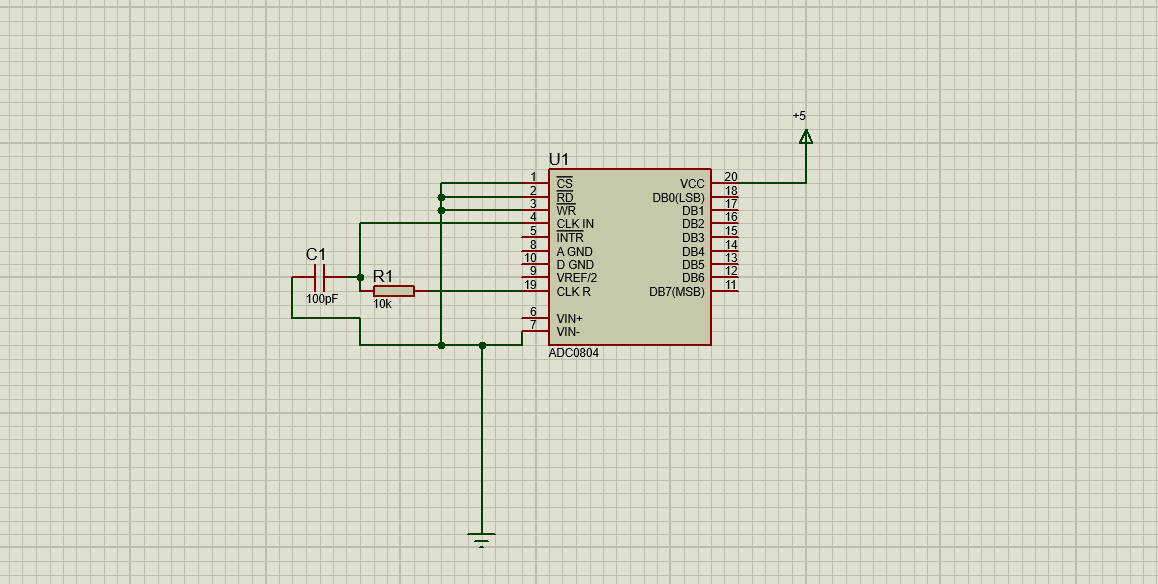
Example Circuit Proteus
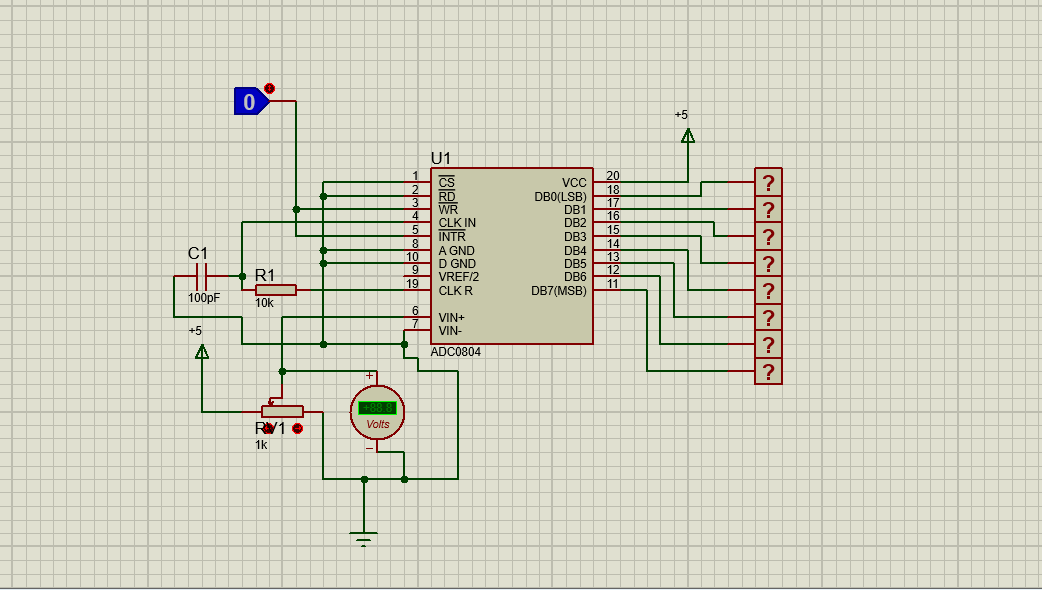
Here is an example circuit of how ADC0804 in proteus. This example circuit could be used to convert the voltages into a digital value. First, complete the basic circuit as mentioned above of ADC0804 and then follow these instructions.
- Attach the variable voltage source with analog pin + and ground with analog pin -ve.
- To control and visualize the output in Proteus use the logic states.
- To control the visualization, attach the logic state changeable with INT and WR pin.
- Attach the logic viewers on the output pins of ADC0804
- Here due to using the same input and output source so the GND of analog and digital will be the same as the power source.
- The Input voltage should not be greater than 6.5 Volts.
- In Proteus, it could work with more than 6.5 Volts but in real life, IC could burn with high voltages easily.
At the end you will get the following circuit:
After completing the circuit run it and see the output.
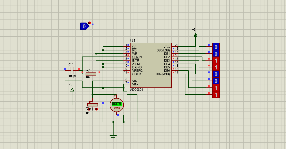
Whenever voltage will be change using variable resistor than it will show the value in Binary form.
Here we are getting the value of “11001100” by giving 4 volts at the input.
Converting binary to Digital:
(11001100) ₂ = (1 × 2⁷) + (1 × 2⁶) + (0 × 2⁵) + (0 × 2⁴) + (1 × 2³) + (1 × 2²) + (0 × 2¹) + (0 × 2⁰) = 204
Analogue value = Step size x Decimal Value
Step Size: When Vref = 5V, for every 19.53mV increase in analogous value cause the increase in one bit on digital side.
Analogue Value = 19.53 x 51 = 393.7mV = 3.9
The actual voltage we are getting after digital conversion is 3.9 and the voltage on the input, we are getting is 4 which is close to the digital voltage. The voltage conversion is the only single example. There are many more applications in real life in which ADC0804 could be used to perform operations. Like temperature sensors, heat sensors, etc. For real example check this article:
Applications
- Widely use with any microprocessor, microcontroller, and ICs.
- It is operated able with microprocessors of 8-bit.
- It could be used to convert the values from the temperature sensor, voltage source and other analog sensors and power sources.
If you want to know about types of ADCs, you can read these articles:
- Tracking Type ADC -Up/Down Counter Analog to Digital Converter
- Counter Type ADC – Staircase Approximation Analog to Digital Converter
- Single Slope and Dual Slope ADC – Integrating Analog to Digital Converter
- Flash ADC: Explained with 3-bit Flash Analog to Digital Converter Example Circuit
- Successive Approximation ADC – Analog to Digital Converter
Other ADC and DAC IC’s: