PIC16F676 is a small-sized pic microcontroller, which is one of the best options for embedded applications. Most of the industrial and home appliances required a small number of pins and small memory space, which can be fulfilled by PIC16F676. It is reliable for student projects due to its high performance which is enhanced due to flash-based technology. PIC16F676 may be smaller in size but it has internal 10-bit Analog to digital converter within a 14-pin package. The PIC Microcontroller also comes in multiple packages and every package consist of 14 pins. The internal flash memory of the microcontroller is 2kb which is excellent for small projects and especially for developing a small program.
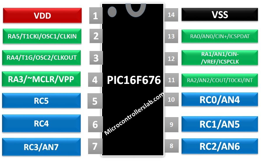
PIC16F676 Pinout Diagram
The pinout diagram is given here. This microcontroller has two GPIO ports PORTA and PORTC. Both these GPIO pins have multiple functions. We will look into the detail of each GPIO pin later in this section.
PIC16F676 GPIO Pins Configuration
Functions and details of all GPIO pins are listed here.
POWER Pins
PIC16F676 has only two input power pins. One is used to give the power supply and the second is used to make the common ground.
- VDD – Pin1
- VSS – Pin14
CRYSTAL/CLOCK Pins
To use the external clock or oscillator with the PIC16F676 there are two pins, one for input and second for output.
- OSC1/CLKIN – Pin2
- OSC2 – Pin3
DIGITAL OUTPUT PINS
In this PIC there are two general-purpose I/O ports A & C, which act as output. Both the ports give the output in the TTL form. The output on these pins won’t be more than VDD. These simple digital outputs can be used only through the program but we will need to specify the port to access the pin of that port. The digital output pins in PIC16F676 are:
- RA0 – GPIO3
- RA1 – GPIO12
- RA2 – GPIO11
- RA4 – GPIO3
- RA5 – GPIO2
- RC0 – GPIO10
- RC1 – GPIO9
- RC2 – GPIO8
- RC3 – GPIO7
- RC4 – GPIO6
- RC5 – GPIO5
INPUT GPIO PINS
In PIC16F676 every pin of both ports A & C can be used as input pins. These pins are TTL based and need to program. These pins have programmable input pull up resistors. The voltage on these pins should not be an increase than VDD. All the input pins are:
- RA0 – GPIO3
- RA1 – GPIO12
- RA2 – GPIO11
- RA4 – GPIO3
- RA5 – GPIO2
- RC0 – GPIO10
- RC1 – GPIO9
- RC2 – GPIO8
- RC3 – GPIO7
- RC4 – GPIO6
- RC5 – GPIO5
INTERUPT PINS
Interrupt pins work like input pins, their basic aim is to get the attention of the controller by neglecting all other functions. It should be described in the program what the controller should do in case of an interrupt. In PIC16F676 there is only one interrupt pin connected to the program counter and require Schematic Trigger (ST) to activate.
- INT – GPIO11
COMPARATOR PINS
PIC16F676 also has a comparator used to compare analog inputs. The single comparator uses three pins, two for input and one for output. The TTL and ST, both inputs can be used on these pins, but the output will always be dependent on the input. The comparator pins in PIC16F676 are:
- COUT – GPIO11 (output)
- CIN – GPIO12 (input 1)
- CIN – GPIO13 (input 2)
TIMER PINS
In PIC16F676 there are two internal timers, and one of the timers has a timer gate which is basically used to control the timer 1 power state. The timer pins of PIC16F676 are:
- T0CKI – GPIO11
- T1CKI –GPIO2
- T1G’ – GPIO3
SERIAL INTERFACE PINS
In this microcontroller, there is a serial communication pin too, but serial communication of these pins will be synchronous and will be mostly used for programming. Three pins will be used, one for data traveling, second for clock pulse and third for voltage. The Pins are:
- ICSPCLK – GPIO12
- ICSPDAT – GPIO13
- VPP – GPIO4
ANALOG INPUT PINS
PIC 16F676 allows the internal ADC channels to convert the analog signal to digital. To convert the analog signal in PIC16F676 has a total of 8 channels which can be used to convert to digital values, 10-bit register is used to store the converted value. The voltage reference pin is used to choose the maximum voltage between VDD and Vref. Here’s all the analog and reference pins:
- AN0 – GPIO13
- AN1 – GPIO12
- AN2 – GPIO11
- AN3 – GPIO3
- AN4 – GPIO10
- AN5 – GPIO9
- AN6 – GPIO8
- AN7 – GPIO7
- Vref – GPIO12
RESET PINS
The PIC comes with only one external reset pin which can be controlled digitally or by an external button. The reset pin is an active low pin and works on ST base logic.
- MCLR’ – Pin4
If you want to start with pic microcontrollers programming in c language or assembly language, you can check this complete guide:
- Pic microcontroller programming in c using Mikroc Pro for PIC
- pic microcontroller assembly language programming
BLOCK DIAGRAM PIC16F676
The internal block diagram of the PIC16F676 is shown below

FEATURES
These features are listed according to the datasheet.
- It gives direct 12 GPIO I/O Pins in a single small package that can be used to drive direct LEDs or other low voltage devices.
- PIC 16F676 has an internal clock that can be used by initializing through the program.
- Automatic sleep ability gives the PIC to save more power.
- Once the code is programmed within, then it will be protected from any theft.
- PIC has 8 analogs to digital converter channels which can store the data of 8-bits.
- It has two internal timers (Timer0 and Timer1). Timer 1 input can be controlled from an external pin.
- PIC16F676 has serial programming pins on it which can be used to program it through two pins.
- IT has an analog comparator that can be used multiple two inputs and their output can be access externally.
PIC16F676 SPECIFICATIONS
- It has standby current is 1nA at 2V and the operating current is 100uA at 2V but the operating voltage varies with the oscillator.
- The internal oscillator of PIC is 4MHz.
- The operating voltage range of PIC16F676 is 2.0 to 5.5V.
- PIC16F676 has 1024 words flash memory, 64 bytes SRAM and 128 bytes EEPROM.
- There are 8 A/D channel but all use a single 10-bit register to store the converted data.
- PIC has an operating temperature range of -40 to 125 degree and it has a storage temperature range of -65 to 150 degrees.
- The maximum CPU speed of the microcontroller is 1MHz.
- The maximum voltage on all pins should not be more than the power pin and current should not be more than 250mA.
PROGRAM MEMORY AND STACK

PIC16F676 APPLICATIONS
- It is used in mostly beginner applications like student projects, development programs, etc.
- Small projects like scrolling display, meters or small LCD also use PIC16F676.
- Those devices which require analog to digital conversion with respect to time or other events use PIC16F676 due to 8 input channels.
Alternative options of pic microcontrollers are PIC16F877A, PIC16F84A, PIC18F46K22
PIC16F676 Peripherals Programming
As mentioned earlier, like other pic microcontrollers, it offers built-in ADC, timers and serial programming features. We explain the registers of these peripherals in this section.
TIMER REGISTER
PIC16F676 has two internal timers register whose values can be manipulated or checked according to the requirement. In this controller the timer0 is 8 bit and has different register as compare to timer1: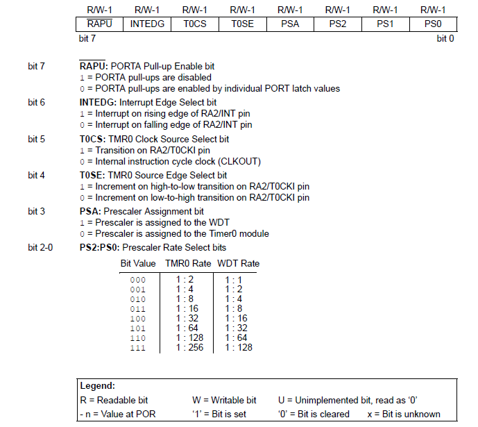
The time1 is a 16-bit timer and comes up with different features and it also has a control pin known as a gate:

ANALOG TO DIGITAL CONVERTER
In Analog to Digital conversion, the data and conversion will be controlled by three registers.
- ANCON0 – Analog to Digital Conversion Register
- ANCON1 – Analog to Digital Conversion Register 1
- ANSEL – Analog Select Register
These three registers will be converting the Analog data to Digital with different status.

The ACON0 will be used to select the data, channel, and reference of the Analog register.

The ANCON1 will be used to select the conversion clock bit of analog to digital. The third bit is the select bit which is used because the analog pins are not only the analog pins they can be used for other functions too. This register will be able to help the controller to use those pins as the analog pin or digital pins.

PIC16F676 INSTRUCTIONS SET ARCHITECTURE
A 14-bit instruction set is used in PIC16F676. The instruction set is categorized into three portions.
Byte-Oriented Operation
In Byte-Oriented the 14-bit instructions set is divided into three parts.
- OPCODE – 7 bits
- Destination – 1 bit
- File Register – 6 bits
Bit Oriented Operation
In Bit-Oriented the instruction set will also be divided into three parts but it has a different number of bits for different operations:
- OPCODE – 7 bits
- Destination – 2 bits
- File Register – 4 bits
Literal and Control Operation
In Literal and Control operation the data will be divided into two parts.
- For Call and GOTO instruction
- OPCODE – 8 bits
- Literal – 6 bits
- For Call and GOTO instruction
- For other instructions
- OPCODE – 11 bits
- Literal – 3 bits
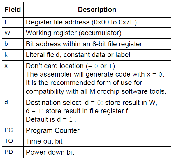
There is some representation for destination, literal and file bit. Here’s the table for representation for each and every available value:
There is also some representation for OPCODE:

The PIC can be programmed easily by using the given instruction and more from the datasheet. This version of PIC can be programmed from different methods too. PIC16F676 only reliable when it has to do some control functions. It won’t be able to perform the smart operations due to its limited design but it is the best option to use as a microcontroller.
good, informative, well organized.