The PIC microcontroller PIC16f877a is one of the most renowned microcontrollers in the industry. This microcontroller is very convenient to use, the coding or programming of this controller is also easier. One of the main advantages is that it can be write-erase as many times as possible because it uses FLASH memory technology. It has a total number of 40 pins and there are 33 pins for input and output. PIC16F877A is used in many pic microcontroller projects. PIC16F877A also have much application in digital electronics circuits.
PIC16f877a finds its applications in a huge number of devices. It is used in remote sensors, security and safety devices, home automation and many industrial instruments. An EEPROM is also featured in it which makes it possible to store some of the information permanently like transmitter codes and receiver frequencies and some other related data. The cost of this controller is low and its handling is also easy. It is flexible and can be used in areas where microcontrollers have never been used before as in microprocessor applications and timer functions etc.
- It has a smaller 35 instructions set.
- It can operate up to 20MHz frequency.
- The operating voltage is between 4.2 volts to 5.5 volts. If you provide it voltage more than 5.5 volts, it may get damaged permanently.
- It does not have an internal oscillator like other PIC18F46K22, PIC18F4550.
- The maximum current each PORT can sink or source is around 100mA. Therefore, the current limit for each GPIO pin of PIC16F877A is 10 mili ampere.
- It is available in four IC packaging such as 40-pin PDIP 44-pin PLCC, 44-pin TQFP, 44-pin QFN
PIN CONFIGURATION AND DESCRIPTION Of PIC16F877A microcontroller
- As it has been mentioned before, there are 40 pins of this microcontroller IC. It consists of two 8 bit and one 16 bit timer. Capture and compare modules, serial ports, parallel ports and five input/output ports are also present in it. This picture shows the pinout diagram of PIC16F877A.
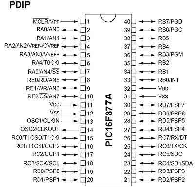
- PIN 1: MCLR: The first pin is the master clear pin of this IC. It resets the microcontroller and is active low, meaning that it should constantly be given a voltage of 5V and if 0 V are given then the controller is reset. Resetting the controller will bring it back to the first line of the program that has been burned into the IC.
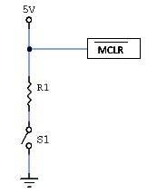
- A push button and a resistor is connected to the pin. The pin is already being supplied by constant 5V. When we want to reset the IC we just have to push the button which will bring the MCLR pin to 0 potential thereby resetting the controller.
- PIN 2: RA0/AN0: PORTA consists of 6 pins, from pin 2 to pin 7, all of these are bidirectional input/output pins. Pin 2 is the first pin of this port. This pin can also be used as an analog pin AN0. It is built in analog to digital converter.
- PIN 3: RA1/AN1: This can be the analog input 1.
- PIN 4: RA2/AN2/Vref- : It can also act as the analog input2. Or negative analog reference voltage can be given to it.
- PIN 5: RA3/AN3/Vref+: It can act as the analog input 3. Or can act as the analog positive reference voltage.
- PIN 6: RA0/T0CKI: To timer0 this pin can act as the clock input pin, the type of output is open drain.
- PIN 7: RA5/SS/AN4: This can be the analog input 4. There is synchronous serial port in the controller also and this pin can be used as the slave select for that port.
- PIN 8: RE0/RD/AN5: PORTE starts from pin 8 to pin 10 and this is also a bidirectional input output port. It can be the analog input 5 or for parallel slave port it can act as a ‘read control’ pin which will be active low.
- PIN 9: RE1/WR/AN6: It can be the analog input 6. And for the parallel slave port it can act as the ‘write control’ which will be active low.
- PIN 10: RE2/CS/A7: It can be the analog input 7, or for the parallel slave port it can act as the ‘control select’ which will also be active low just like read and write control pins.
- PIN 11 and 32: VDD: These two pins are the positive supply for the input/output and logic pins. Both of them should be connected to 5V.
- PIN 12 and 31: VSS: These pins are the ground reference for input/output and logic pins. They should be connected to 0 potential.
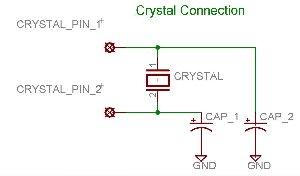
- PIN 13: OSC1/CLKIN: This is the oscillator input or the external clock input pin.
- PIN 14: OSC2/CLKOUT: This is the oscillator output pin. A crystal resonator is connected between pin 13 and 14 to provide external clock to the microcontroller. ¼ of the frequency of OSC1 is outputted by OSC2 in case of RC mode. This indicates the instruction cycle rate.
- PIN 15: RC0/T1OCO/T1CKI: PORTC consists of 8 pins. It is also a bidirectional input output port. Of them, pin 15 is the first. It can be the clock input of timer 1 or the oscillator output of timer 2.
- PIN 16: RC1/T1OSI/CCP2: It can be the oscillator input of timer 1 or the capture 2 input/compare 2 output/ PWM 2 output.
- PIN 17: RC2/CCP1: It can be the capture 1 input/ compare 1 output/ PWM 1 output.
- PIN 18: RC3/SCK/SCL: It can be the output for SPI or I2C modes and can be the input/output for synchronous serial clock.
- PIN 23: RC4/SDI/SDA: It can be the SPI data in pin. Or in I2C mode it can be data input/output pin.
- PIN 24: RC5/SDO: It can be the data out of SPI in the SPI mode.
- PIN 25: RC6/TX/CK: It can be the synchronous clock or USART Asynchronous transmit pin.
- PIN 26: RC7/RX/DT: It can be the synchronous data pin or the USART receive pin.
- PIN 19,20,21,22,27,28,29,30: All of these pins belong to PORTD which is again a bidirectional input and output port. When the microprocessor bus is to be interfaced, it can act as the parallel slave port.
- PIN 33-40: PORT B: All these pins belong to PORTB. Out of which RB0 can be used as the external interrupt pin and RB6 and RB7 can be used as in-circuit debugger pins.
Note: All pins have multiple functionalities. Like PORTC pins can be used as digital input pins, digital output pins, for UART communication, I2C communication. But, we can use one function of each port at a time or you have to program it smartly so that you can switch between different functionalities. Like once you need one pin to read analog signal, define it for analog purpose and then switch to other functions like digital output etc. For beginners, we suggest to use one pin for single functionality and you can use multi-function mode, once you become an expert in programming.
HOW TO PROGRAM THE INPUT AND OUTPUT PORTS
- As we have studied 5 input and output ports namely PORTA, PORTB, PORTC, PORTD and PORTE which can be digital as well as analog.
- We will configure them according to our requirements. But in case of analog mode, the pins or the ports can only act as inputs. There is a built in A to D converter which is used in such cases. Multiplexer circuits are also used.
- But in digital mode, there is no restriction. We can configure the ports as output or as input. This is done through programming. For PIC the preferable compiler is mikro C pro which can be downloaded from their website.
- There is a register named as ‘TRIS’ which controls the direction of ports. For different ports there are different registers such as TRISA, TRISB etc.
- If we set a bit of the TRIS register to 0, the corresponding port bit will act as the digital output.
- If we set a bit of the TRIS register to 1, the corresponding port bit will act as the digital input.
- For example to set the whole portb to output we can write the program statement as:
TRISB=0;- Now the port will act as the output port and we can send any value on the output such as
PORTB=0XFF;- FF represents all 1’s in binary i.e. FF=11111111, now all the pins of port b are high. If we connect LEDs at all the pins then they will all start glowing in this condition.
- If we want to negate the values of the port b we can use the statement:
PORTB=~PORTB;- Now all the pins of the port b will be low.
Compiler for PIC16F877A microcontroller
- Three popular compiler which are used to program pic microcontrollers are MPLAB XC8, Mikro C for pic, PIC CCS compiler and Hi-Tech compiler.
- The official compiler is MPLAB XC8 compiler which is developed by manufactures of PIC16F877A.
- We generally recommend Mikro C for pic compiler for beginners and MPLAB XC8 compiler for those who want to learn pic microcontrollers programming from register level bare metal concepts.
- You can go through our list pic microcontroller compilers article for further details.
Main features of PIC16F877A microcontroller
Like all other microcontroller, PIC16F877A also provide built-in useful features as mentioned in this list:
- Analog to digital converter module : It has 8 bit ADC module which consists of 8 channels. We can use 8 analog sensors with this microcontroller.
- Timers: It provides three timers timer0, timer1 and timer2. All these timers can be used either in timer mode or in counter mode. These timers are used to generate delays, pulse width modulation, counting external events and timer interrupts. TIMER0 is a 8 bit timer and it can operate with internal or external clock frequency. When we use Timer0 in timer mode, we usually operate it with internal frequency and in counter mode, we trigger it with external clock source. Similarly, TIMER1 is a 16-bit timer and it can also operate in both modes. TIMER2 is also of 8-bit. It is used with PWM as a time base for CCP module.
- EEPROM : It also has built-in Electrically erasable read only memory 256 x 8 bytes which can used to store data permanently even if the microcontroller is switched off, data will remain there. It is usually used with electronics lock related projects.
- PWM modules : It also provide 2 CCP modules. CCP stands for capture compare PWM modules. We can easily generate two PWM signals with this microcontroller. The maximum resolution it supports is 10 bits. you can read PWM using PIC16F877A microcontroller tutorial for more information and programming.
- Serial or UART communication pins : It support one UART channel. UART pins are used for serial communication between digital devices. RC7 pin is a transmitter or RX pin which is pin number 26. RC6 is a receiver or Tx pin which is pin number 25. For additional details, check this complete guide on serial communication using pic16f877a microcontroller.
- I2C Communication : PIC16F877A also support I2C communication and its has one module for I2C communication. Pin#18/RC3 and 23/RC4 are SCL and SDA pins respectively. SCL is a serial clock line and SDA is serial data line. I2C communication tutorial will help you understand further.
- Interrupts : Interrupts have wonderful applications in embedded systems field. If you don’t know about interrupts, I suggest you to get complete understanding about them, you will not get command on embedded programming them. PIC16F877A microcontroller provides 8 types of interrupts namley; External interrupts, timer interrupts, PORT state change interrupts, UART interrupt, I2C, PWM interrupts. you can read this guide on pic microcontroller interrupts for additional information.
- Comparator module : It has a comparator module which composed of two comparators. They are used for comparison of analog signal similar to comparators in electronics circuits. Input pins for these comparators are RA0, RA1, RA2 and RA3 and output can measured through RA4 and RA5.
- Watchdog timer : WDT is a on chip separate oscillator which runs freely. It is a separate oscillator from OSC1/CLKI. WDT will also work even if the device is in sleep mode. It is used to wake up device from sleep mode and also used to generate watchdog timer reset.
- Sleep mode : PIC16F877A also provide sleep mode operation. In this mode, device operates at very low power. All peripherals draws minimum amount of current. Wake up from sleep mode from interrupts resources like timer1 interrupt, uart interrupt, EEPROM write completion operation and many others.
- Brown out detection : It also has a brown out detection circuit which detects the significant drop in power supply voltage. If supply voltage drop from a certain limit, it will generate a interrupt signals. This configuration bit (BODEN) is used to disable or enable this circuitry.
- Brown out reset : This option reset the device upon detection of brown out interrupt signal from BODEN signal. if supply voltage goes below threshold for more than 100 micro seconds,
- Programmable code protection, Brown out reset will occur and device will remain reset until the voltage raise to its nominal value. Device checks for voltage after every 72ms.
Some other momentous features are listed below :
- Power on Reset
- Multiple oscillator group
- In-Circuit Debugger
- In-Circuit Serial programming
- Low voltage ICSP programming
CODE TO LIGHT UP A SINGLE LED/ FLASHING LED
This is simple tutorial on blinking an LED with PIC16F877A microcontroller. We use Mikro C for pic compiler to write this code. If you are just getting started with pic microcontroller programming, you can check this tutorial on Mikro C for pic:
- Writing your first program using Mikro C for pic compiler
- Pic microcontroller programming in c using Mikro c for pic
void main()

 {

      TRISB.F0 = 0  // the direction of RB0 is set as output

                 //or TRISB = 0xFE (0xFE = 11111110)

      do // setting the infinite loop

      {

        PORTB.F0 = 1; // setting the RB0 pin to high

        Delay_ms(500); // delay of 500 milli seconds

        PORTB.F0 = 0; // setting the RB0 pin to low

        Delay_ms(500); // again a delay of 500 milli seconds

     }while(1);

 }
This code is used to toggle PORTC pin number zero with the delay of five hundred mili seconds. Inside the main function this line initialize the RB0 as digital output pin.
TRISB.F0 = 0After that do while loop is used, because we want to toggle LED again and again. Inside the do while loop, these line make the RB0 digital high for 500ms.
PORTB.F0 = 1; // setting the RB0 pin to high
Delay_ms(500); // delay of 500 milli seconds
And similarly these lines, turn off the LED for 500ms.
PORTB.F0 = 0; // setting the RB0 pin to low
Delay_ms(500); // again a delay of 500 milli seconds
Circuit diagram for flashing LED WITH PIC16F877A
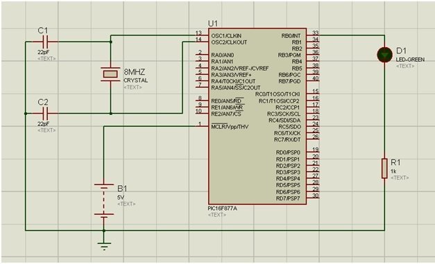
- Design this circuit in proteus. Connect the pins with the source, ground and oscillator as explained in the pin description section.
- Connect 8MHz oscillator with OSCI and OSC2 through two 22 pico farad capacitors.
- Provide 5 volt to Reset pin through 10k ohm resistor. Resistor is not shown in simulation, but you should connect resistor while making circuit practically.
- An LED is connected on pin 33 RB0, a resistor is used to limit the current and to prevent the LED from burning up. Write and compile the program in mikro C pro.
- Burn the microcontroller with the hex file by double clicking on the controller in proteus and run the circuit successfully. best way to learn any microcontroller is to check its data sheet.
- Pic kit3 is a famous programmer used to upload code to microchip chips, How to program using Pic kit3 is a good source to read.
you may also like to read tutorials on PIC16F877A microcontroller
- LED blinking with pic16f877a microcontroller
- LCD interfacing with pic16f877a microcontroller
- keypad interfacing with pic16f877a microcontroller
- serial communication using pic16f877a microcontroller
- timers of pic16f877a microcontroller
- interrupts
- stepper motor interfacing
- servo motor interfacing with pic16f877a
- dc motor interfacing with pic16f877a
- Complete list of pic microcontroller tutorials
Sir,
can u please provide the code to interface Bluetooth with pic 16f877A? It would be of great help sir.
This tutorial is wonderful,i like it. Sir,can i get assembling language programming on this. My e-mail is perek4u@yahoo.co.uk
sir, i want to get the hex code for automatic microcontroller based irrigation system using pic16f877a microcontroller and soil moisture sensor.
excellent
Please kindly provide the code to interface light dependent resistor (LDR) with Pic 16f877A. …also send it to my email . My email is hamisbaba@yahoo.com. Thank you.
Thanks very much for the useful tutorials
Thank you very much for the turtorial I have been able to clear many uncleared. Please sir I need to know the difference memory map and data sheet. My mail Bubaabdul26@yahoo.com
so useful for a beginner
it is very useful for a fresher
very good
because of in simple words, it is easily understand
Sir plz give me program for automatic power factor correction using pic16f877a..
With complete circuit diagram..
chandansharma261@gmail.com
If you want to purchase code and circuit diagram contact me at microcontrollerslabhub@gmail.com
Sir can u help me wih coding
please help me i went to do real time crops field monitoring system by plc16f778A micro control use by protues
CAN You please help in calculating instataneous voltage and current through sampling
Sir plz give me program for a gas or smoke detection alarm using pic 16f877a and the mq2 gas sensor
Sir,
I have a doubt , whether the pin6 in port A is RA0 or RA4 and where is the timer0
given.
it is very useful for our projects
nice explination
it is very useful for my examination purpose
thank you
Sir what is R IN RA0 OF the pin diagram what does it stand for…?
It’s so useful, great notes to study embedded programming using microcontroller.
Thank you.
sir I need the code for the automatic bell
In PIC 16F877A, What is ‘A’ stands for?
It’s so useful, great notes to study
embedded programming using
microcontroller.
Thank you. excuse ,please help me the c-code of low cost home security using pic16F877A and gsm network on email gebeyawmollaw30@gemail.com
How do you program this controller in c+ language? How do we interface this microcontroller with a 555 timer, LDR,
thanks
The diagram of the pin 1 reset circuit is wrong.
R1 should be between the 5V supply and the junction to pin 1 (MCLR).
Feel free to delete this if you correct it.
I came here for the pinouts so thanks for that anyway.
Bob.
Yeah, I saw that too. Maybe he’s testing us to see if we’re paying attention.
Hello,
I want to make a project IOT BASED UNDERGROUND CABLE FAULT DETECTOR
How I will be done it using PIC16F877A
I mean which will be the code of this microcontroller?