Recommended Components
The following parts and reference books are useful for building and learning 8051 microcontroller projects.
| Component | How it’s used in your 8051 projects | Buy on Amazon |
|---|---|---|
| AT89S52 (8051) microcontroller | A modern, in-system-programmable 8051-core MCU that runs the code in these tutorials. | Check Price |
| USBasp programmer (ISP) | Burns the compiled HEX file into the AT89S51/AT89S52 over the ISP header. | Check Price |
| Breadboard | Solderless base for wiring the 8051 and the project’s components. | Check Price |
| Jumper Wires | Make the connections between the MCU, components and power rails. | Check Price |
| Book: The 8051 Microcontroller & Embedded Systems (Mazidi) | The classic 8051 textbook — architecture, assembly & C programming with interfacing examples. | Check Price |
| Book: The 8051 Microcontroller, 3rd Ed. (Ayala) | A popular reference covering 8051 architecture, programming and applications. | Check Price |
As an Amazon Associate we earn from qualifying purchases. Prices and availability are accurate as of the date/time indicated and are subject to change.
EEPROM
Electrically Erasable Programmable Read Only Memory (EEPROM pronounced as “double E prom) is like a ROM but data can be erased from it electrically without removing it from the computer. Data is created in them by electrical pulses and a grid. We can also change the data in it according to our requirement, to erase a certain data we don’t have to erase the prom completely like in a regular rom. A basic ROM chip can only be programmed once whereas an EEPROM can be programmed again and again.
Categories of EEPROM Devices
There are two main categories of EEPROM devices:
SERIAL BUS
This type works in different phases. Address phase, data phase and op-code phase are the three phases in which this chip functions. Some of the common types of serial interfacing are UNI/O, 1-wire, SPI, microwire and I2C.
PARALLEL BUS
For total handling of memory it has a wide address bus and also a data bus consisting of 8 bits. Parallel built in eeprom is present in many microcontrollers.

OPERATING PRINCIPLE OF EEPROM:
The characteristics of a cell will be modified by the electrons. These electrons are trapped inside a gate known as floating gate. So now the storage will be in form of logic 1 or logic 0.
There are two transistors in most of the cells:
- Storage transistor.
- Access transistor.
The storage transistor traps the electrons as it consists of the floating gate (floating gate is a transistor that can hold an electrical charge). And in the operation, access transistor is used. As soon as the electrons leave the floating gate, a cell is erased in case of EPROM, but in EEPROM if the electrons are trapped in floating cell then the cell will be erased
EEPROM INTERFACING WITH MICROCONTROLLERS
The interfacing of EEPROM with microcontrollers is mostly done through I2C. I2C is known as the master-slave protocol. There are two signals of I2C, a clock signal and a data signal. Clock signal SCL is controlled by the Master. The transfer of data occurs through the manipulation of clock signal. The same clock controls all the slaves connected with the master. The figure below shows the interfacing with microcontrollers:
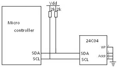
We can connect a number of slave devices with the master IC. Every slave has a unique address, the master device also contains an address. The slave device could be an LCD, a keyboard, a clock, a thermometer or a memory interface. The I2C controller used here will work as a master device and the EEPROM will act as slave. A set of control signals is sent for read or write operations. These control signals include address bits and data bits. Proper clock signals accompany these control signals.
INTERFACING OF AT24C02 EEPROM WITH 8051
AT24C02 is a serial EEPROM by ATMEL. It consists of two wire 2k bits. There are 8 bit addresses used for the addressing of memory. The memory is so organized that in a single byte 256 words are present, these are arranged in 32 pages and each page contains 8 bytes.Let us take a circuit which demonstrates the interfacing of 8051 microcontroller with AT24C02. The microcontroller will perform a write operation and then it will read it also. The results will be displayed on LCD.
PIN DESCRIPTION OF 24C02 EEPROM
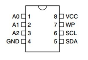
The pin description of 24C02 is given below:
- A0-A2:
The first three pins are the address pins. As in a system multiple devices can be connected therefore they need proper addressing. These address pins are either connected with the source Vcc or with the ground permanently in a circuit. In this specific circuit the address is ‘000’ because all the pins are connected to ground.
- GND:
This pin must be connected to ground or 0 potential. It is the 4th pin of the IC.
- SDA:
SDA is the serial data pin. It is a bidirectional pin. The data and the control bits are serially read or write through this pin. It is the 5th pin of the IC.
- SCL:
SCL is the clock signal pin. For the transmission of data from the SDA pin a clock signal is required for each bit transfer. A negative edge transfers data from the EEPROM and a positive edge carries the data to the EEPROM. It is the 6th pin of the IC.
In the circuit, the bit 0 of port P1 is connected to SDA and pin 1 of port P1 is connected to SCL.
- WP:
It is the Write Protect pin. If a high signal is given to it, the IC is protected from any write operation. And if a low signal is given to it, then the read and write operations are allowed normally. It is the 7th pin of the IC.
For the normal working, the WP pin is connected to ground in the circuit.
- Vcc:
Vcc is the DC power supply for the 24C02. It is the 8th pin that must be connected to 5V. Without this DC supply, the IC will not work.
The device addressing scheme of 24C02 is shown in the figure below. It consists of 8 bits (1 byte). The first 4 bits are fixed sequence bits, then the next 3 bits are the address bits which indicate the address of the device and finally the last bit indicates whether a read or a write operation is to be performed.

EEPROM INTERFACING WITH CONTROLLER in STEPS
The following steps describe the interfacing and data transmission:
START CONDITION:The start condition initiates the read or write operation. The SCL should be high and the SDA should transit from high to low, when this condition occurs then the EEPROM gets the signal that controller is ready. At the end of start condition the SCL signal becomes low because the transmission of data occurs when the SCL signal transits from low to high.

TRANSFER OF BITS TO EEPROM:
One bit at a time is transferred to the EEPROM when the clock signal SCL goes from low to high. Now the SDA pin becomes the input and receives the bits. The data should not change when the SCL is high because the device will interpret it as a start or a stop condition. However the data can be changed when SCL is low.

Similarly the bits can be transferred from EEPROM when the SCL transits from high to low. In this case the SDA pin becomes the output pin.
ACKNOWLEDGEMENT BIT:
The EEPROM send a 0 to the controller when it receives a word successfully. This acknowledgement bit is read by the controller when it sends a 1-0 transition at SCL. This bit should be checked after the transmission of every word.
READ/ WRITE OPERATIONS:
In each read or write operation, a fixed set of words is to be transferred to or from the EEPROM. When the read or write operation is finally completed, a stop signal is sent which indicates that the process is now completed.

STOP CONDITION:
After the successive transmission of all the data, a stop condition will be generated by the master. The SCL should transit from low to high and then it should remain high, while the SDA transits from low to high, to define the stop condition.

The figure below shows how microcontroller is interfaced with EEPROM. An lcd displays the output results.
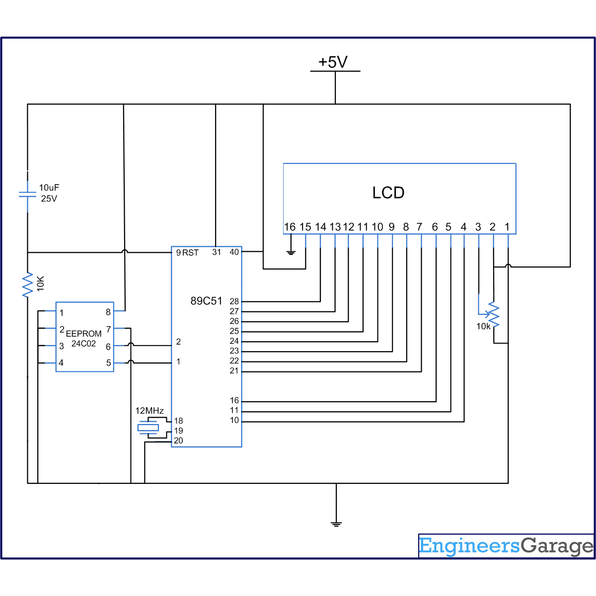
The circuit diagram shows the complete connections between 24C02 and 89C51. A 12MHz crystal is also connected between then pin 18 and 19 to provide the clock for the functioning of microcontroller. The address pins of 24C02 have been grounded to give the address ‘000’. Vcc of 5V is given at the 8th pin and the pins SDA and SCL are connected to the microcontroller for the transmission of data and clock signals.
A SECURITY DOOR LOCK CIRCUIT using EEPROM

This is another circuit which shows the interfacing between 89C51 and 24C02. An lcd and a keypad have also been interfaced with the 8051 microcontroller. The keypad is used to enter the number or the password and an LCD displays the status. A desired password has already been stored by the user in the 24C02. Now when he wants to open the lock he enters the password by the keypad. This password should match with the password stored in the EEPROM. If the password is correct then the door will be opened.
Photo Credits:
EEPROM INTERFACING by engineersgarage
INTERFACING WITH MICROCONTROLLERS by pantechsolutions
- Parallel device by elprocus
what is the address of this eeprom to communicate over I2C ??
0x50
please give the asm code for password door lock with eeprom
our team can write a code for you in 50$ if you are interested to purchase contact us at microcontrollerslabhub@gmail.com