In this tutorial, we will learn to use STM32 Nucleo timer in PWM mode to generate PWM signals and how to configure them to generate signals with different duty cycle and frequency. We will use an LED dimmer example to demonstrate how to setup the timer in PWM mode using STM32Cube IDE and HAL libraries along with a comprehensive guide about the PWM mode. At the end, we will show you a demo where we will control LED brightness by giving a variable duty cycle signal to an LED.
As discussed earlier, we will be using STM32CubeIDE, therefore, you should have the latest version installed on your system. You can follow this guide to install it:
STM32 Nucleo Timer PWM Mode
The Nucleo STM32F103RB comes with four timers known as TIM1, TIM2, TIM3, and TIM4. They act as a clock and are used to keep track of time based events. The timer module can work in different configurations such as timer mode, counter mode, PWM mode, output compare mode etc. This guide focuses on configuring the timer module in PWM mode.
When configuring the STM32 Nucleo timer module in PWM mode, an internal clock source clocks the timer module and generates a digital waveform (PWM signal) on the output channel pin. The value of the output compare register which is OCR is continuously monitored and matched with the increasing values of the Timer register. At the particular moment when both the values are same, the state of the output pin is toggled until the end of the period. This occurs repeatedly.
What exactly happens is that when the timer gets clocked, the timer counter counts till the auto reload value. When the value is reached, the state of the output channel pin is set HIGH. When the timer counter counts till the CCRx register vale, the state of the output channel pin is set LOW as a match occurs. The timer counter starts again and the process repeats continuously.
The PWM signal has a specific frequency set by the internal clock, prescaler and the TIMx_ARRx register, duty cycle held in the channel CCRx register value and resolution. The TIMx_CCRx register controls the duty cycle and the frequency is correlated with the PWM resolution. Let us look at all these features in detail.
A PWM signal has three properties which are of utmost importance. This includes the frequency of the signal, its duty cycle and the resolution.
STM32 PWM Frequency
To set a particular frequency of the PWM signal, the ARR value, prescaler value and the frequency of the internal clock are used. The frequency of the output PWM signal can be calculated as follows:
F(pwm) = F(clk) / (ARR+1)(PSC+1)
To get your desired output PWM frequency, the user sets the prescaler and internal clock frequency and finds the ARR value that will generate the required PWM frequency.
STM32 PWM Duty Cycle
The CCRx register is responsible for controlling the duty cycle percentage of the PWM signal. This value is calculated by CCRx/ ARR to find the duty cycle percentage value.
STM32 PWM Resolution
The resolution of the PWM signal is also an important aspect of the output signal that is generated. It sets the number of discrete duty cycle levels which means the number of steps it takes for the duty cycle to get to the maximum number set. This step size can be calculated by using the frequency of the internal clock and the PWM signal.
PWM Resolution = log( F(clk)/F(pwm) )/ log(2)
The table below shows how the PWM resolution varies with different frequencies of the PWM signal for a STM32 Nucleo 16 bit timer with clock frequency of 72 MHz.
| PWM Resolution (bits) | Approximate PWM Frequency |
| 16 | 1.1 kHz |
| 14 | 4.4 kHz |
| 12 | 17.5 kHz |
| 10 | 70 kHz |
| 8 | 281 kHz |
| 6 | 1.125 MHz |
| 4 | 4.5 MHz |
There is another formula as well which involves the ARR value instead of the frequencies. You can use this formula as well to achieve the desired PWM resolution in bits.
PWM Resolution in bits = log(ARR+1)/ log(2)
STM32 Nucleo Timer PWM Output Channels
As mentioned previously, the STM32 Nucleo consists of four timer where each timer has multiple channels that can be configured. This allows the user to set up multiple PWM signals with varying duty cycles by using the same timer. As the timer will be same, therefore all the PWM signals generated like this will be synchronized.
The figure below shows the main circuit for capture channel 1.

As you may see in the circuit above, the capture channel consists of a capture register with a shadow register, an input stage consisting of a digital filter, a multiplexer, and Prescaler for capturing, and an output stage consisting of output control and a comparator. Here the output stage is responsible for creating a reference waveform.
PWM Modes
The PWM mode (mode 1 or mode 2) can be configured separately for each output channel. Therefore, each OCx output can have a PWM signal associated with it. The mode is selected by writing the OCxM bits which are present in the TIMx_CCMRx register. For PWM mode 1 bits ‘110’ are written and for PWM mode 2, bits ‘111’ are written. The OCxPE bit present in the TIMx_CCMRx register and the ARPE bit present in the TIMx_CR1 register is enabled by the user according to the particular preload register and the auto preload register respectively.
When setting the timer module operation in counter mode, there are different counting modes the user can choose from. This includes the up-counting/down-counting (edge aligned) and center aligned mode etc.
Edge Aligned Mode
The edge aligned mode consists of configurations where the PWM mode may be set up in up-counting or down-counting mode.
As seen in the figure below for edge aligned waveforms, the reference PWM signal which is known as OCxREF has a HIGH state when TIMx_CNT is less than TIMx_CCRx. When this condition is not met, its state goes to LOW. Moreover, when the compare value in TIMx_CCRx register has a value greater than the auto-reload value held in TIMx_ARR register then the refence PWM signal stays HIGH. Otherwise, if the compare value is 0 then it stays LOW.
Note that in both PWM modes, either 1 or 2, the values TIMx_CNT and TIMx_CCRx are matched to check which value (TIMx_CNT or TIMxCCRx) is lesser than equal the other, according to the direction of the counter set.

Center Aligned Mode
In case of center aligned mode, the compare flag may be set according to different counting ways (count up, count down or count up and down). This counter’s counting mechanism depends on the configuration of the CMS bits in the TIMx_CR1 register. In the figure below, you can view the center aligned PWM signals where TIMx_ARR=8 in PWM mode 1.

STM32 Nucleo PWM Mode LED Dimmer Project
Let’s create and build a project in STM32 CubeIDE where we will configure a timer in PWM mode and control the brightness of an LED connected at the timer channel output pin. We will configure Timer 2 in PWM mode where channel 1 will be set as PWM generation channel 1. The brightness of the LED will increase as the duty cycle varies from 0 to 100% and then decreases again from 100% to 0% and the process repeats continuously.
Open the CubeIDE and head over to a new project.
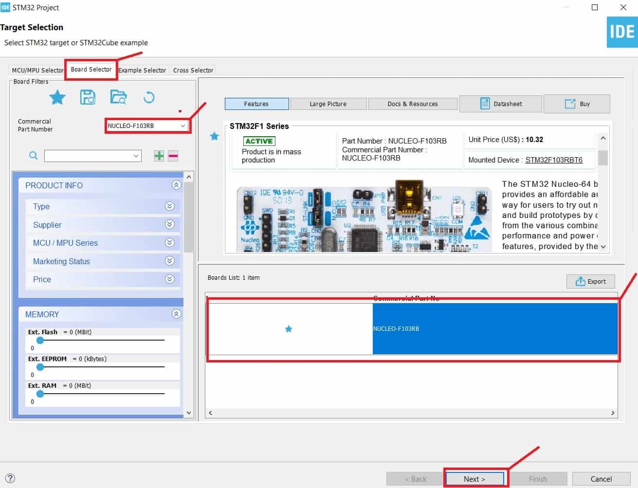
Then for the target selection, specify the STM32 Nucleo board number. After that click on any column as shown in the picture below. Then click the ‘Next’ button.
Specify the name of your project then click ‘Finish’ to complete the setup of your project.
Setup Timer in PWM Mode
Now head over to Timers to configure the timer to work in PWM mode. We have selected Timer2. The mode for Timer2 is set next where we configure the clock source as the internal clock and Channel 1 as PWM Generation CH1. This way Timer2 will work in PWM mode where PA0 (Timer2 Channel 1) will be set as an output. Now go to the Parameter Settings and set the counter settings. The counter period (ARR value) is set as 65535 which is the maximum. The auto-reload preload is enabled. The timer mode is set as PWM mode 1.

Note that the resolution is set as 16 bits and the frequency of the output PWM signal is 1098.6Hz which can be easily calculated through the F(pwm) formula discussed previously.
Go to System Core > RCC then select ‘Crystal/Ceramic Resonator’ in from the High Speed Clock feature.
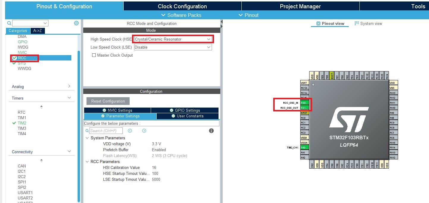
Now we have enabled the RCC external clock source.
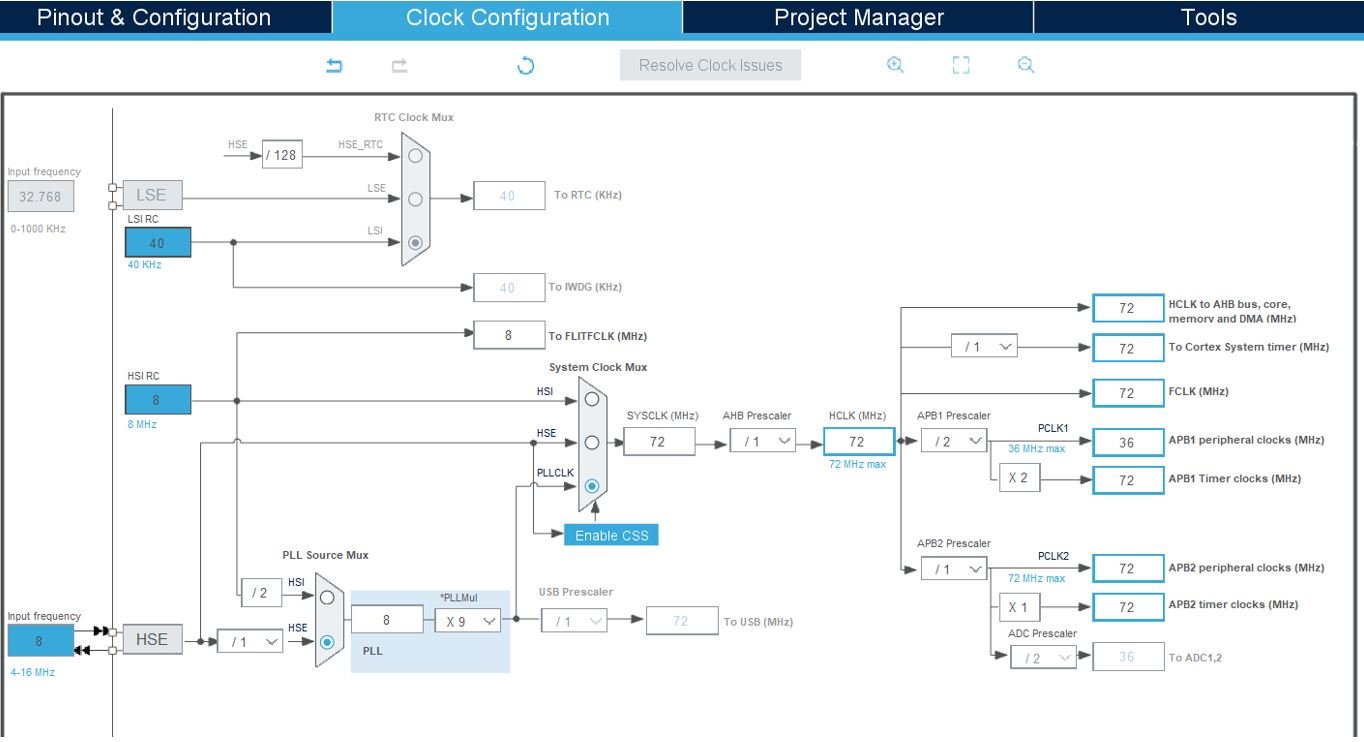
Clock Configuration
Next go to the Clock Configuration found at the top. This will open the following window. Here we will select the clock frequency.
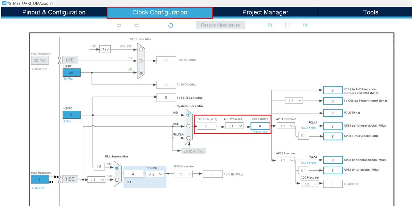
You can specify your system clock. We will set it as 72 MHz. These are the configurations we have set:
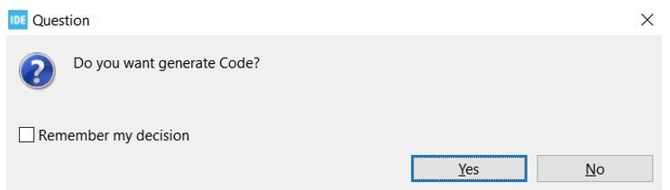
Now we will save our file. Press Ctrl + S. The following window will appear. Click ‘Yes.’ This will generate a template code for you.
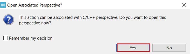
Another window will appear that will ask if you want to open the perspective. Click ‘Yes.’
STM32 Nucleo LED Dimmer Code
We will set up a code in which the duty cycle is varied by writing the value to the CCR1 register.
Now let us look at our main.c file that was generated. Inside the main.c file, make sure the following code is part of your script by including the lines of code given below.
#include "main.h"

TIM_HandleTypeDef htim2;

void SystemClock_Config(void);
static void MX_GPIO_Init(void);
static void MX_TIM2_Init(void);

int main(void)
{
  int32_t dutyCycle = 0;
  HAL_Init();

  SystemClock_Config();

  MX_GPIO_Init();
  MX_TIM2_Init();

  HAL_TIM_PWM_Start(&htim2, TIM_CHANNEL_1);

  while (1)
  {
	   while(dutyCycle < 65535)
	        {
	            TIM2->CCR1 = dutyCycle;
	            dutyCycle += 100;
	            HAL_Delay(2);
	        }
	        while(dutyCycle > 0)
	        {
	            TIM2->CCR1 = dutyCycle;
	            dutyCycle -= 100;
	            HAL_Delay(2);
	        }
  }

}
Working of the Code
First we create a variable called ‘duty_cycle’ which initially holds the value 0. Then we initialize all the configured peripherals and set the system clock configuration. After that we start the PWM signal generation by calling HAL_TIM_PWM_Start() function. This function takes in two parameters. The first parameter is the pointer to the TIM_HandleTypeDef structure that holds the configuration parameters for the timer module. The second parameter is the timer channel that will be enabled. It can take either of the values listed below:
- TIM_CHANNEL_1: TIM Channel 1 is enabled
- TIM_CHANNEL_2: TIM Channel 2 is enabled
- TIM_CHANNEL_3: TIM Channel 3 is enabled
- TIM_CHANNEL_4: TIM Channel 4 is enabled
HAL_TIM_PWM_Start(&htim2, TIM_CHANNEL_1);Inside the infinite while() loop, we will run two while loops that will write the timer2 value to the CCR1 register which holds the duty cycle. The duty cycle will vary from 0 to 100% as its value is increased/decreased by 100 in each loop, that will alter the brightness of the LED according to the duty cycle.
  while (1)
  {
	   while(dutyCycle < 65535)
	        {
	            TIM2->CCR1 = dutyCycle;
	            dutyCycle += 100;
	            HAL_Delay(2);
	        }
	        while(dutyCycle > 0)
	        {
	            TIM2->CCR1 = dutyCycle;
	            dutyCycle -= 100;
	            HAL_Delay(2);
	        }
  }
main.c file
This is how a complete main.c file will be after modification.
/* USER CODE BEGIN Header */
/**
  ******************************************************************************
  * @file           : main.c
  * @brief          : Main program body
  ******************************************************************************
  * @attention
  *
  * Copyright (c) 2024 STMicroelectronics.
  * All rights reserved.
  *
  * This software is licensed under terms that can be found in the LICENSE file
  * in the root directory of this software component.
  * If no LICENSE file comes with this software, it is provided AS-IS.
  *
  ******************************************************************************
  */
/* USER CODE END Header */
/* Includes ------------------------------------------------------------------*/
#include "main.h"

/* Private includes ----------------------------------------------------------*/
/* USER CODE BEGIN Includes */
#include <stdio.h>
/* USER CODE END Includes */

/* Private typedef -----------------------------------------------------------*/
/* USER CODE BEGIN PTD */

/* USER CODE END PTD */

/* Private define ------------------------------------------------------------*/
/* USER CODE BEGIN PD */
/*
volatile uint8_t state = IDLE;
volatile uint8_t message[35] = {'\0'};
volatile uint32_t T1 = 0;
volatile uint32_t T2 = 0;
volatile uint32_t ticks = 0;
volatile uint16_t TIM2_OVC = 0;
volatile uint32_t frequency = 0;
*/
/* USER CODE END PD */

/* Private macro -------------------------------------------------------------*/
/* USER CODE BEGIN PM */

/* USER CODE END PM */

/* Private variables ---------------------------------------------------------*/
TIM_HandleTypeDef htim2;

/* USER CODE BEGIN PV */

/* USER CODE END PV */

/* Private function prototypes -----------------------------------------------*/
void SystemClock_Config(void);
static void MX_GPIO_Init(void);
static void MX_TIM2_Init(void);
/* USER CODE BEGIN PFP */

/* USER CODE END PFP */

/* Private user code ---------------------------------------------------------*/
/* USER CODE BEGIN 0 */

/* USER CODE END 0 */

/**
  * @brief  The application entry point.
  * @retval int
  */
int main(void)
{
  /* USER CODE BEGIN 1 */
	int32_t dutyCycle = 0;
  /* USER CODE END 1 */

  /* MCU Configuration--------------------------------------------------------*/

  /* Reset of all peripherals, Initializes the Flash interface and the Systick. */
  HAL_Init();

  /* USER CODE BEGIN Init */

  /* USER CODE END Init */

  /* Configure the system clock */
  SystemClock_Config();

  /* USER CODE BEGIN SysInit */

  /* USER CODE END SysInit */

  /* Initialize all configured peripherals */
  MX_GPIO_Init();
  MX_TIM2_Init();
  /* USER CODE BEGIN 2 */
  HAL_TIM_PWM_Start(&htim2, TIM_CHANNEL_1);
  //HAL_TIM_IC_Start_IT(&htim2, TIM_CHANNEL_1);
  /* USER CODE END 2 */

  /* Infinite loop */
  /* USER CODE BEGIN WHILE */
  while (1)
  {
	  while(dutyCycle < 65535)
		{
			TIM2->CCR1 = dutyCycle;
			dutyCycle += 100;
			HAL_Delay(2);
		}
		while(dutyCycle > 0)
		{
			TIM2->CCR1 = dutyCycle;
			dutyCycle -= 100;
			HAL_Delay(2);
		}
    /* USER CODE END WHILE */

    /* USER CODE BEGIN 3 */
  }
  /* USER CODE END 3 */
}

/**
  * @brief System Clock Configuration
  * @retval None
  */
void SystemClock_Config(void)
{
  RCC_OscInitTypeDef RCC_OscInitStruct = {0};
  RCC_ClkInitTypeDef RCC_ClkInitStruct = {0};

  /** Initializes the RCC Oscillators according to the specified parameters
  * in the RCC_OscInitTypeDef structure.
  */
  RCC_OscInitStruct.OscillatorType = RCC_OSCILLATORTYPE_HSE;
  RCC_OscInitStruct.HSEState = RCC_HSE_ON;
  RCC_OscInitStruct.HSEPredivValue = RCC_HSE_PREDIV_DIV1;
  RCC_OscInitStruct.HSIState = RCC_HSI_ON;
  RCC_OscInitStruct.PLL.PLLState = RCC_PLL_ON;
  RCC_OscInitStruct.PLL.PLLSource = RCC_PLLSOURCE_HSE;
  RCC_OscInitStruct.PLL.PLLMUL = RCC_PLL_MUL9;
  if (HAL_RCC_OscConfig(&RCC_OscInitStruct) != HAL_OK)
  {
    Error_Handler();
  }

  /** Initializes the CPU, AHB and APB buses clocks
  */
  RCC_ClkInitStruct.ClockType = RCC_CLOCKTYPE_HCLK|RCC_CLOCKTYPE_SYSCLK
                              |RCC_CLOCKTYPE_PCLK1|RCC_CLOCKTYPE_PCLK2;
  RCC_ClkInitStruct.SYSCLKSource = RCC_SYSCLKSOURCE_PLLCLK;
  RCC_ClkInitStruct.AHBCLKDivider = RCC_SYSCLK_DIV1;
  RCC_ClkInitStruct.APB1CLKDivider = RCC_HCLK_DIV2;
  RCC_ClkInitStruct.APB2CLKDivider = RCC_HCLK_DIV1;

  if (HAL_RCC_ClockConfig(&RCC_ClkInitStruct, FLASH_LATENCY_2) != HAL_OK)
  {
    Error_Handler();
  }
}

/**
  * @brief TIM2 Initialization Function
  * @param None
  * @retval None
  */
static void MX_TIM2_Init(void)
{

  /* USER CODE BEGIN TIM2_Init 0 */

  /* USER CODE END TIM2_Init 0 */

  TIM_ClockConfigTypeDef sClockSourceConfig = {0};
  TIM_MasterConfigTypeDef sMasterConfig = {0};
  TIM_OC_InitTypeDef sConfigOC = {0};

  /* USER CODE BEGIN TIM2_Init 1 */

  /* USER CODE END TIM2_Init 1 */
  htim2.Instance = TIM2;
  htim2.Init.Prescaler = 0;
  htim2.Init.CounterMode = TIM_COUNTERMODE_UP;
  htim2.Init.Period = 65535;
  htim2.Init.ClockDivision = TIM_CLOCKDIVISION_DIV1;
  htim2.Init.AutoReloadPreload = TIM_AUTORELOAD_PRELOAD_ENABLE;
  if (HAL_TIM_Base_Init(&htim2) != HAL_OK)
  {
    Error_Handler();
  }
  sClockSourceConfig.ClockSource = TIM_CLOCKSOURCE_INTERNAL;
  if (HAL_TIM_ConfigClockSource(&htim2, &sClockSourceConfig) != HAL_OK)
  {
    Error_Handler();
  }
  if (HAL_TIM_PWM_Init(&htim2) != HAL_OK)
  {
    Error_Handler();
  }
  sMasterConfig.MasterOutputTrigger = TIM_TRGO_RESET;
  sMasterConfig.MasterSlaveMode = TIM_MASTERSLAVEMODE_DISABLE;
  if (HAL_TIMEx_MasterConfigSynchronization(&htim2, &sMasterConfig) != HAL_OK)
  {
    Error_Handler();
  }
  sConfigOC.OCMode = TIM_OCMODE_PWM1;
  sConfigOC.Pulse = 0;
  sConfigOC.OCPolarity = TIM_OCPOLARITY_HIGH;
  sConfigOC.OCFastMode = TIM_OCFAST_DISABLE;
  if (HAL_TIM_PWM_ConfigChannel(&htim2, &sConfigOC, TIM_CHANNEL_1) != HAL_OK)
  {
    Error_Handler();
  }
  /* USER CODE BEGIN TIM2_Init 2 */

  /* USER CODE END TIM2_Init 2 */
  HAL_TIM_MspPostInit(&htim2);

}

/**
  * @brief GPIO Initialization Function
  * @param None
  * @retval None
  */
static void MX_GPIO_Init(void)
{
/* USER CODE BEGIN MX_GPIO_Init_1 */
/* USER CODE END MX_GPIO_Init_1 */

  /* GPIO Ports Clock Enable */
  __HAL_RCC_GPIOD_CLK_ENABLE();
  __HAL_RCC_GPIOA_CLK_ENABLE();

/* USER CODE BEGIN MX_GPIO_Init_2 */
/* USER CODE END MX_GPIO_Init_2 */
}

/* USER CODE BEGIN 4 */


/* USER CODE END 4 */

/**
  * @brief  This function is executed in case of error occurrence.
  * @retval None
  */
void Error_Handler(void)
{
  /* USER CODE BEGIN Error_Handler_Debug */
  /* User can add his own implementation to report the HAL error return state */
  __disable_irq();
  while (1)
  {
  }
  /* USER CODE END Error_Handler_Debug */
}

#ifdef  USE_FULL_ASSERT
/**
  * @brief  Reports the name of the source file and the source line number
  *         where the assert_param error has occurred.
  * @param  file: pointer to the source file name
  * @param  line: assert_param error line source number
  * @retval None
  */
void assert_failed(uint8_t *file, uint32_t line)
{
  /* USER CODE BEGIN 6 */
  /* User can add his own implementation to report the file name and line number,
     ex: printf("Wrong parameters value: file %s on line %d\r\n", file, line) */
  /* USER CODE END 6 */
}
#endif /* USE_FULL_ASSERT */
Building the Project
Save the main.c file after modifying it. Now we are ready to build our project.
To build our project press Ctrl + B or go to Project > Build All.
Your project will start building. After a few moments, your project will be successfully built if there are no errors.
Demonstration
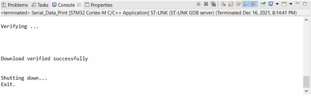
Next press the RUN button in the IDE. The ‘Edit configuration’ window will open up. Click ‘OK’.
After a few moments, the code will be successfully sent to the STM32 board.
Otherwise, press the RESET button on your STM32 board.
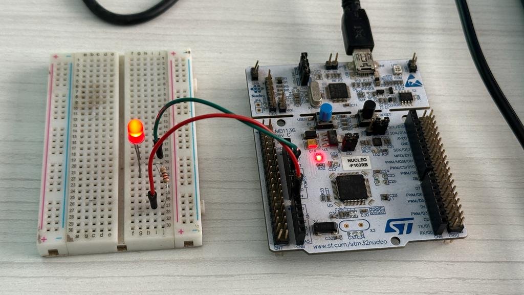
Hardware Setup for STM32 Nucleo LED Dimmer
For this project we will require the following components:
- STM32 Nucleo
- One 5mm LED
- One 220 ohm current limiting resistor
- Connecting Wires
- Breadboard
Connect the components as shown in the schematic diagram below:
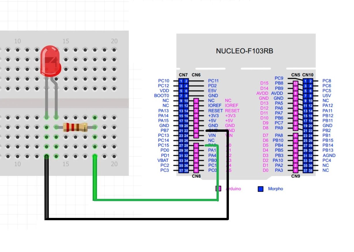
Connect the LED’s anode pin to PA0 through a 220-ohm resistor. The cathode pin will be grounded.
Press the Reset button of STM32. The brightness of the LED increases from 0 to 100% then decreases from 100% to 0. The process repeats endlessly.
Conclusion
In summary, this tutorial has effectively demonstrated how to configure an STM32 Nucleo timer to operate in PWM mode using STM32CubeIDE and HAL libraries. By walking through the setup of a simple LED dimmer project, we’ve seen how changing the duty cycle can control the brightness of an LED. Moreover, it provided insight into several aspects of a PWM signal, such as frequency, duty cycle, and resolution, along with their practical applications.
You may also like to read: