AD620 is low cost instrumentation amplifier capable of producing highly accurate results. Commercial versions available in the market are 8-pin SOIC and DIP packages. The gain can be adjusted up to 10,000 by the incorporation of only a single resistor. This Low cost power amplifier is ideal for use in precision data acquisition. AD620 consumes very less power i.e. maximum supply current can merely be around 1.3mA. The super beta processing in the input stage keeps the input bias current low. Low noise and very low value of input bias current render its suitability for medical devices. It’s compactness, high efficiency, and low power consumption makes it possible to be used for portable devices and applications. AD620 acts as an efficient pre-amplifier due to low input voltage noise.
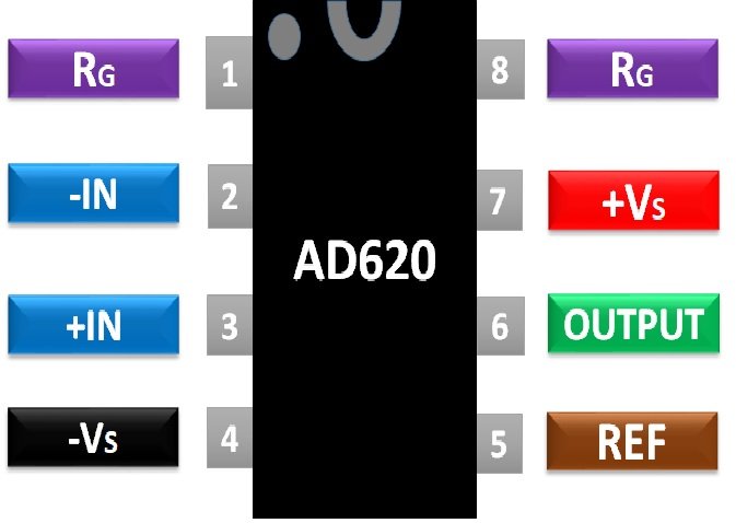
AD620 Pinout Diagram
The PDIP (N), CERDIP (Q) and SOIC (R) packages come as 8-pin variants. The general pin configuration and details of all pins are given in this section as per the datasheet.
| PINS | Details |
|---|---|
| 1 Gain Adjustment Resistor ( ) | This pin is for attaching gain adjustment resistor-terminal one |
| 2 (Inverting Input -IN) | This pin is for applying inverting input voltage |
| 3 (Non-Inverting Input +IN) | This pin is for applying non-inverting input voltage |
| 4 (Negative Supply Voltage ) | This pin is for applying negative supply voltage |
| 5 (Reference REF) | This pin is meant for reference voltage |
| 6 (Output Voltage OUTPUT) | This pin is for obtaining output voltage |
| 7 (Positive Supply Voltage ) | This pin is for applying positive supply voltage |
| 8 Gain Adjustment Resistor ( ) | This pin is for attaching gain adjustment resistor-terminal two |

AD620 Electrical Features and Specifications
AD620 ensures gain adjustment by the use of a single external resistor. The low power consumption is one of the key features of AD620. Other equivalents of AD620 are AD620A, AD620B AD620S. The comparison of their features is listed in this table. For more features and electrical specifications of Power Instrumentation Amplifier download datasheet given in the last section.
| Parameters | AD620A | AD620B | AD620S |
|---|---|---|---|
| Gain Range | 10,000 | 10,000 | 10,000 |
| Gain Error G=1 (%) | 0.10 | 0.02 | 0.10 |
| Gain Error G=1000 (%) | 0.7 | 0.5 | 0.7 |
| Input Offset (µV) | 125 | 50 | 125 |
| Input Bias current (nA) | 2.0 | 1.0 | 2.0 |
| Input Offset Current (nA) | 1.0 | 0.5 | 1.0 |
| Input Voltage Range (V) | + -1.2 | + -1.2 | + -1.2 |
| Input offset current (nA) | 200 | 50 | 500 |
| Input Impedance Differential Common Mode (GΩ_pF) | 10II2 | 10II2 | 10II2 |
| Common Mode Rejection Ratio G=1 (dB) | 90 | 90 | 90 |
| Common Mode Rejection Ratio G=1000 (dB) | 130 | 130 | 130 |
| Slew Rate (V/µs) | 1.2 | 1.2 | 1.2 |
| Small Signal -3dB Bandwidth G=1 (kHz) | 1000 | 1000 | 1000 |
| Small Signal -3dB Bandwidth G=1000 (kHz) | 12 | 12 | 12 |
| Settling Time to 0.01% G= 1-100 (µs) | 15 | 15 | 15 |
| Settling Time to 0.01% G= 1000 (µs) | 150 | 150 | 150 |
| Input Voltage Noise (nV/ Hz) | 13 | 13 | 13 |
| Output Voltage Noise (nV/ Hz) | 100 | 100 | 100 |
| Reference Input Resistance (kΩ) | 20 | 20 | 20 |
| Reference Input Current (µA) | 60 | 60 | 60 |
| Reference Input Voltage Range (V) | + -1.6 | + -1.6 | + -1.6 |
| Output Short Circuit Duration | Indefinite | Indefinite | Indefinite |
| Lead Temperature Range for 10sec soldering (°C) | 300 | 300 | 300 |
| Operating Temperature Range (°C) | -40 to +85 | -40 to +85 | -55 to +125 |
Other l amplifiers are LM4871, LM709, LM201
Where and How to Use Low Power Instrumentation Amplifier IC
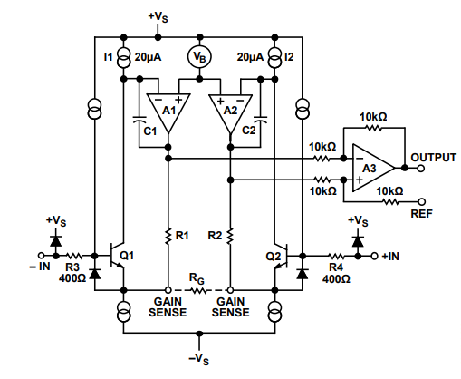
The schematics diagram of AD620 shows that it uses 3 Op-Amp approaches to attain highly accurate output. Again adjustment resistance is connected between pin no. 1 and 8. The value of this resistance RG will determine the exact value of gain to be attained. The two are related as RG = 49.4kΩ/ (G-10). However for attaining G=1, pins 1 and are left open or unattended. Supply voltage is applied at pin no 4 and 7. The reference terminal or pin 5 provides zero volt reference and can be used to insert offset up to 2V if the load ground differs from system one. Pin 2 receives inverting input and pin 3 non-inverting. The output is obtained at pin no 6. A simplified schematic of AD620 is being added for reference. In short, the gain for a given value of RG can be calculated by this equation:
G = (49.4 kΏ / RG) + 1
AD620 Amplifier Examples
The most common but vital example circuits using AD620 are medical ECG equipment and blood pressure monitor. These circuits are included to show the effective use of AD620.
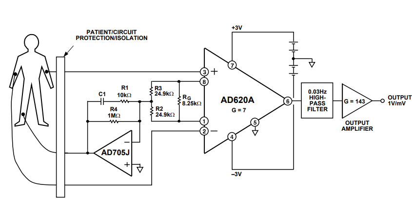
Medical ECG Circuit Example

Pressure Monitor Circuit Example
If you want to explore more about this IC of Power Instrumentation Amplifier, Download datasheet:
Applications
The real-life applications of AD620 are:
- Blood Pressure Monitor
- Medical ECG
- Weigh Scales
- Data Acquisition Equipment
- Process Controls in Industry
- Battery operated and portable Devices