CD40103 or CD40103 is 8-bit synchronous down counter which belongs to a CMOS based logic family. It consists of a single output pin that is CO/ZD. This pin gives high output when counter reachers zero value. It has control inputs and one output which is Carry out or Zero Detect. All these inputs and output are active-low logic. It is cascadable in both synchronous and ripple mode.
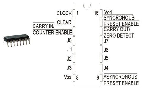
CD40103 IC Pinout Diagram
This is a pinout diagram of cd40103 8-bit down counter.
Pin Configuration Details
It has 16 pins in total having different functions. This tables lists all pins along with their functions.
| Pin Name | Description |
|---|---|
| CLOCK | Enabling and Disabling of clock signal. |
| CLEAR | Clear the counter to its maximum count. |
| CARRY-IN/COUNTER ENABLE | It is a carry-input pin also known as counter enable pin. When this input pin is HIGH, counter stops counting. |
| J0, J1, …, J7 | Jam inputs representing an 8-bit binary word |
| VDD | Connect with Positive terminal of power supply |
| Vss | Connect with Grounf terminal |
| CARRY-OUT/ZERO-DEFECT | Output pin whose value would be LOW remains in the same state for one complete clock cycle if carry-in input is active low |
| SYNCHRONOUS PRESET-ENABLE | Preset the counter synchronously. |
| ASYNCHRONOUS PRESET-ENABLE | Preset the counter asynchronously |
CD40103 Features
- Synchronous or asynchronous preset
- Operates at medium speed with a clock frequency (fCL)= 3.6 MHz at VDD= 10V
- Can be cascaded for designing more than 8-bit counter
- The maximum value of input current at 18V = 1 µA
- Wide voltage supply range of 3 to 15V with different noise margins according to temperature
- One output can drive up to 50 inputs.
- Inputs are provided with diodes protection which interfaces inputs to voltages by using current limiting resistors when Vcc is in excess.
- Standardized, symmetrical output characteristics
- Parametric ratings: 5V, 12V and 15V
How and Where to Use CD40103 Down Counter?
The value in counter decrements by one on every positive edge of a clock signal. The counter resets itself to its maximum value that is 255 in decimal. In such case, CD40103 down counter ignores the singal of any input pin. Furthermore, when the CLEAR input is low. It has two preset enables.
If the digital state of synchronous preset-enable pin is active low, input signal at carry input pin becomes don’t care. Therefore, data available on pins J0-J7 passes to a counter as soon as positive edge of clock happens. On the other hand, When asynchronous preset-enable input pin is low, data at the JAM inputs is asynchronously forced into the counter and it is independent of the state of clock signal, carry-input or synchronously preset enable pin.
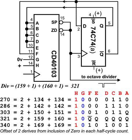
Cascading Example CD40103 Counter
It can be cascaded using the carry in and Carry out pins to design a 16 bit or more than 8 bits counter. Cascading can be done in either synchronous or ripple mode. This IC can be used in many ways for example counting the number of revolutions of wheel by connecting a sensor with wheel. Sensor will send the pulses to this IC and this IC will count the pulses which can also be used to find the speed of wheel.
Divisor Example
Applications
CD4103/CD4012 have huge arread of applications. Some of them are:
- We can use it to design Interrupt timers.
- CD40102 can also use to implement Programmable counter/timer. It is a flexible microprocessor peripheral that measure voltage transitions by counting the number of edges that occur on an input signal.
- This device has two basic applications which are counting events and measuring time. Events counting is also possible through this IC.
- In Central Processing Units, counters performs program instructions execution one by one. Program Counter is also its application.
- We can design digital divisor circuits and Digital clocks