The CD4012 is a dual 4-input NAND gate IC based on CMOS technology. In other words, it has two NAND gates and each NAND gate has 4 input pins. Both logic gates can operate independently. It belongs to the CD4000 series of integrated circuits that require low power consumption and have wide voltage supply ranges. The voltage supply range for this IC is from 3V to 15V. Small fluctuations in the voltages are tolerated. It has 2 independent NAND gates having four inputs. The operating temperature range for this IC is from – 55 °C to + 125 °C. It is available in 14-pin packages of PDIP, GDIP, PDSO.
Recommended Components
The following parts are used in this article, along with a generic electronics kit that is handy for building and testing the circuit.
| Component | How it’s used | Buy on Amazon |
|---|---|---|
| CD4012 dual 4-input NAND gate | The CD4012 dual 4-input NAND gate IC this article covers. | Check Price |
| Electronic component assortment kit (1390 pcs) | A handy assortment of resistors, capacitors, LEDs, diodes and transistors for building circuits. | Check Price |
| Digital multimeter (AstroAI) | Measures voltage, current, resistance and checks continuity while you build and debug. | Check Price |
| Breadboard | Solderless base for prototyping the circuit. | Check Price |
| Jumper Wires | Make the connections on the breadboard. | Check Price |
As an Amazon Associate we earn from qualifying purchases. Prices and availability are accurate as of the date/time indicated and are subject to change.
CD4012 Pinout Diagram
This dual 4-input NAND IC has 14 pins. Pin A1, B1, C1, D1 are input pins for one gate. Similarly, A2, B2, C2, D2 are input pins for the other one. Q1 and Q2 are output pins. This figure shows the pinout diagram of CD4022.
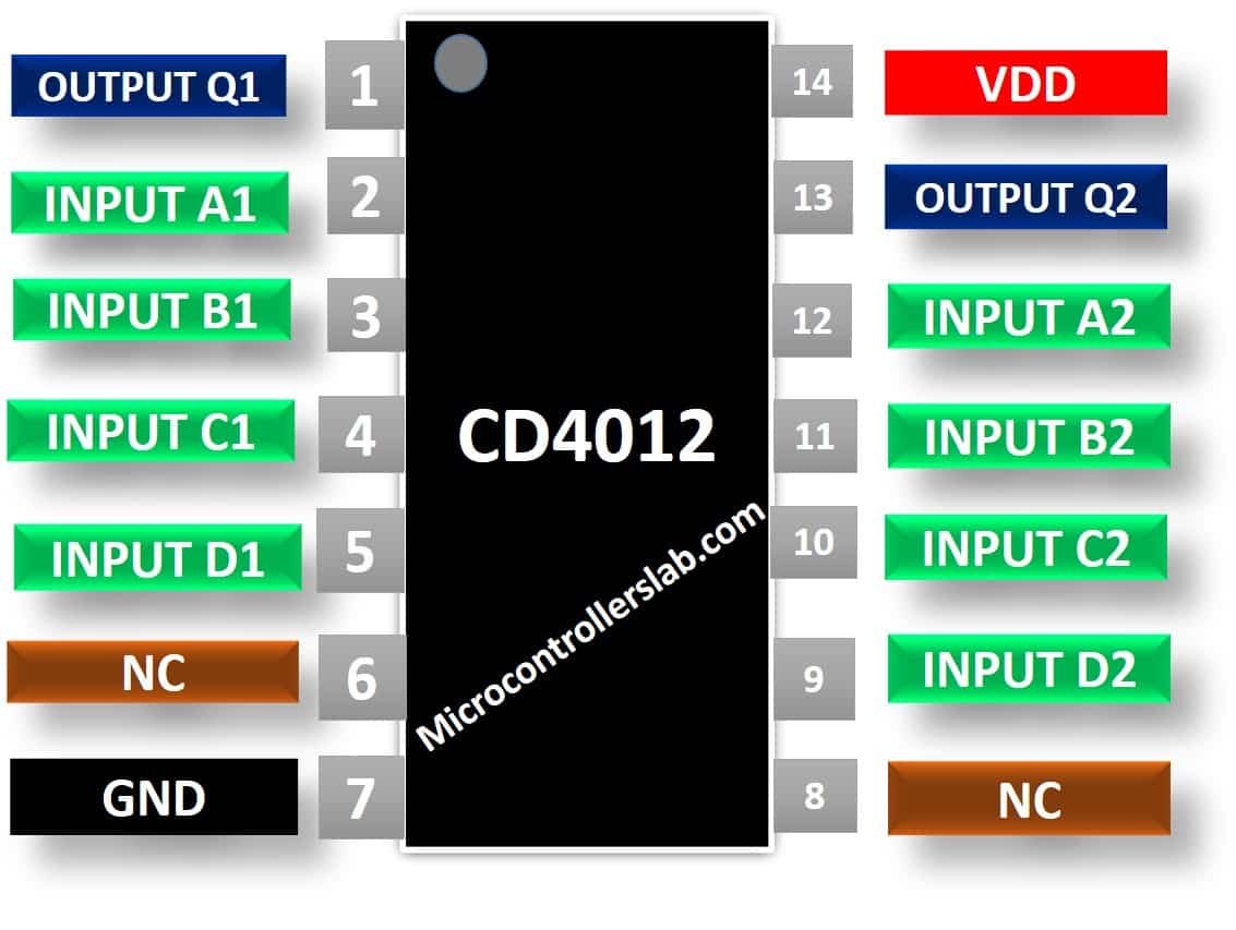
CD4012 Pins Description
The CD4012 IC has total 14 pins. All the pins, their names, and description are given in the table below:
| Pin Number | Pin Name | Description |
|---|---|---|
| 1 | Q1 | Output of NAND gate 1 |
| 2,3,4,5 | A1, B1, C1, D1 | Four inputs of NAND gate 1 |
| 6, 8 | NC | Not Connected |
| 7 | GND | Negative power supply or ground of the circuit |
| 9, 10, 11, 12 | A2, B2, C2, D2 | Four Inputs of NAND gate 2 |
| 13 | Q2 | Output of NAND gate 2 |
| 14 | Power supply of 5V |
CD4012 NAND Gate Features
- Dual NAND gate IC with an operating voltage range of 3 V to 15 V
- Buffered inputs and outputs with operating voltage of typically 5V
- Power Dissipation: 500mW
- Diode protection on all inputs
- Propagation Delay for at 10V is 50ns (maximum)
- Minimum logic low and logic high voltage is from 0.05V to 4.95V
Where and how to use it
The operation of CD4012 IC is quite simple. A NAND gate is opposite of AND gate. It gives logic HIGH, when any of its input value is LOW and when both of its inputs are HIGH, it gives LOW logic at the output. Let us suppose that we have a NAND gate with A and B as its inputs and X as its output. The truth table for this gate is given in the table below. The logic expression will be:
X =~(A.B)
| A | B | X |
|---|---|---|
| 0 | 0 | 1 |
| 0 | 1 | 1 |
| 1 | 0 | 1 |
| 1 | 1 | 0 |
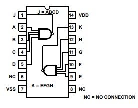
CD4012 Internal Structure
CD4012 IC is a dual NAND gate IC. Its operation is just like the 2 input NAND gate IC. All you need to do is connect pin 8 of the IC with the negative power supply or ground of the circuit and pin 16 with positive voltage supply. Switch on the power supply. The functional diagram of IC showing the internal connections is given below.
By applying different combinations at the input pins, you will receive an output value whose voltage will be equal to the operating voltage. You can observe the effect on the output in the table below.
| Inputs | Output | |||
|---|---|---|---|---|
| A | B | C | D | Q |
| 0 | 0 | 0 | 0 | 1 |
| 0 | 0 | 0 | 1 | 1 |
| 0 | 0 | 1 | 0 | 1 |
| 0 | 0 | 1 | 1 | 1 |
| 0 | 1 | 0 | 0 | 1 |
| 0 | 1 | 0 | 1 | 1 |
| 0 | 1 | 1 | 0 | 1 |
| 0 | 1 | 1 | 1 | 1 |
| 1 | 0 | 0 | 0 | 1 |
| 1 | 0 | 0 | 1 | 1 |
| 1 | 0 | 1 | 0 | 1 |
| 1 | 0 | 1 | 1 | 1 |
| 1 | 1 | 0 | 0 | 1 |
| 1 | 1 | 0 | 1 | 1 |
| 1 | 1 | 1 | 0 | 1 |
| 1 | 1 | 1 | 1 | 0 |
The values for both NAND gates will be same. In this gate as there are four inputs, therefore the logic expression would be:
Q = ~(A.B.C.D)
Simulation Example Circuit
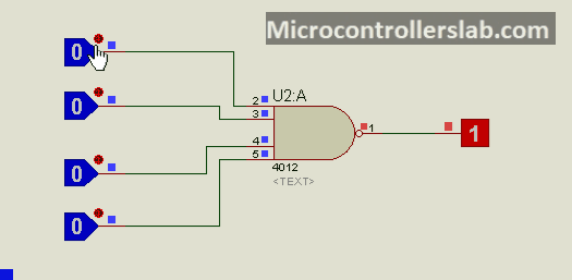
As it is a universal gate, therefore it can also be used with other logic gates. You can use this IC in such applications that require multiple gates or buffer circuits. It is normally used in projects and applications where low dissipation and high noise immunity are required. It is also used for digital implementation in logic circuits.
Proteus Simulation
CD4012 Applications
This IC has numerous applications in electrical circuits. Few are mentioned below:
- Digital Logic circuits for producing desired logical function
- Encoders, Decoders, Multiplexers and De-multiplexers
- Universal gate and can be with NOT gate to perform functions of all other gates. This reduces hardware and cost
- Logic Buffer circuits
- Oscillators, Networking and Digital Systems
2 Dimension Diagram

DataSheet
Other Logical Gates: