CS51411 IC is a low voltage, 1.5 Ampere buck regulator IC. We can use it to step down the voltage meanwhile stepping up the current from input to output. It operates at a fixed frequency of 260kHz and 520kHz. Additionally, it supports external biasing and synchronization function. It takes the input voltage in a range of 4.5V to 40V and steps down the voltage giving output in a range of 1.27V to 40V. Other Equivalent options are CS51412, CS51413, CS51414.
CS51411 Pin Configuration Diagram
This picture depicts the pinout diagram along with details of each pin.
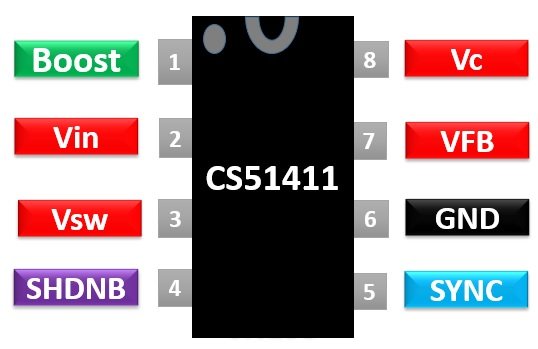

Pin Description
Pin#01: BOOST
The BOOST pin provides an additional driving voltage to the base of the power transistor inside a chip. This would decrease the switch-on voltage thus leading to reduced power dissipation and increased efficiency. The boost pin voltage should not exceed 40V.
Pin#02: Vin
This the input pin where an input voltage signal is applied.
Pin#03: Vsw
It is connected internally to the emitter of the NPN transistor and provides an output to an inductor connected at this pin externally.
Pin#04: SHDNB
It is a TTL compatible active low pin. When this pin is low, the IC enters into a sleep mode by reducing supply current to the 20 and the power transistor remains off. In normal operation, it is left unconnected.
Pin#05: SYNC
It is the input pin used for synchronization.
Pin#06: GND
This pin is connected of the ground of the circuit.
Pin#07:
The feedback voltage pin is connected to the negative pin of the error amplifier in chip. It is used to protect the IC from short circuits or severe over currents by limiting the current value.
Pin#08: Vc
It is the output of the error amplifier and input of the PWM comparator.
CS51411 Features
The features of CS51411 are enlisted below:
- It has an architecture that provides efficient regulation, simplified design, and ultrafast transient response.
- The output current of 1.5A.
- synchronization function for parallel supply operation and minimizing noise.
- It has a BOOST input pin which maximizes the efficiency and minimizes power dissipation by allowing Bootstrapped operation.
- Maximum Quiescent current is 6250
- It has a shutdown pin which provides a power-down option in case of overvoltages and short circuits. During power-down condition, the quiescent current is reduced to 85A.
- It has a soft start feature and thermal shutdown protection.
Where to use it?
The CS51411 IC is a buck regulator having a high operating frequency along with a wide input and output voltage range. You can use this IC in portable devices for stepping down voltages. It has small size, performs efficient regulation and has a built-in protection circuitry against under voltages, overcurrent and frequency foldback. Therefore, you can use these in applications where you need a buck converter with these specifications.
Due to its high switching frequency and accuracy, it is used to provide power in applications involving signal switching and multiplexing.
Alternative Options:
How to use it CS51411 Buck Regulator?
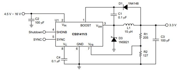
A simple circuit diagram is given to explain its operation. A capacitor of 0.1µF is connected at the BOOST input pin for maintaining voltage. Input voltage is applied at pin 2. The capacitor of 100µF connected at this pin which absorbs the AC components of an input signal and removes the ripple current. An inductor is connected at pin 3. Inductor value should be carefully selected. If you need to reduce the physical size of the inductor, then chose a lower value of the inductor. Inductors of higher value reduce core losses and cut down the ripple currents. In most of the applications, the inductor value lies in the range of 2.2 H and 22 H.
CS51411 Applications
Some of the applications of CS51411 Buck converter includes:
- Telecommunications
- Portable devices
- High-speed data applications
- Powering all types of Digital signal processors
- Blood Gas Analysers
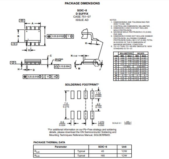
2D Diagram
The two-dimensional diagram of the 8-pin SOIC package of IC CS51411 is given below. For detail about other packages, refer to the datasheet.