TL081 is a high-speed operational amplifier integrated circuit consisting of a high voltage JFET and bipolar transistor. It has low input bias currents, trimmed input offset voltage, and high slew rates. Furthermore, it is pin-compatible with the LM741 IC and is used in electronics and computers, etc. Additionally, the range of its operations is compatible with both common-mode and differential voltage range applications.
Pinout Diagrams
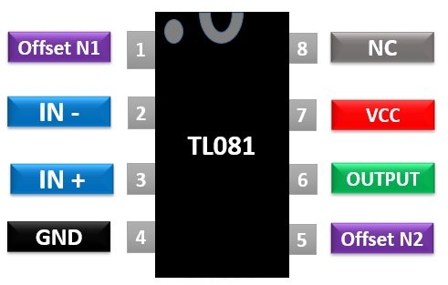
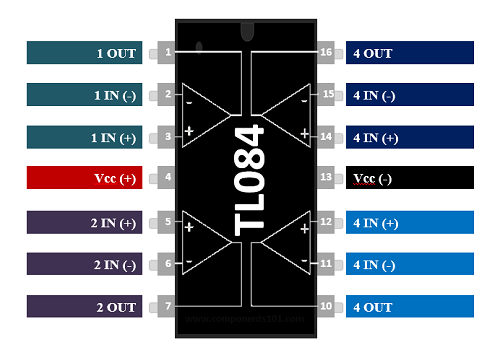
As you can depict from the pinout diagram that this JFET input operational amplifier IC has only one op-amp inside a chip, unlike TL074. Similarly, Equivalents, ICs such as TL082, TL084 have similar electrical features and specifications except for a number of op-amps inside a single package.
- TL082: Dual Op-Amp
- TL084: Quad Op-Amp
TL081 Pinout
TL082 Pinout
TL084 Pinout
Pin Configuration Description
The TL081 is a general-purpose op-amp IC consisting of 8 pins whose functionalities are described in the table below:
| Pin no. | Pin Name | Description |
|---|---|---|
| 1, 5 | OFFSET N1, OFFSET N2 | Input offset adjustment pins |
| 2 | IN- | Inverting Input of op-amp |
| 3 | IN+ | Non-inverting terminal |
| 4 | Vcc- | Ground or Negative power supply |
| 6 | OUT | Output pin of op-amp |
| 7 | Vcc+ | Positive power supply |
| 8 | NC | Not Connected |
TL081/TL082, TL084 Features
- Wide common-mode Rejection ratio of 70dB to 86dB and wide voltage supply range
- A low input bias current
- less Power Requirement
- Internal frequency compensation
- Supply current is 1.4mA which is very low
- Low offset current
- No requirement of a latch
- High input impedance JFET input stage
- short-circuit protection for output
- a large gain bandwidth of 3MHz
- high input impedance
- Slew rate is high typically 16 V/µs
- Operating temperature range is from –55 °C to +125 °C
Where to use it?
The TL081IC can be used in all those applications requiring a high slew rate, low input bias current and offset voltage and wide bandwidth. As it is an op-amp IC, therefore, it is used in voltage followers, ac to dc conversions, sample and hold circuits, high-speed integrators. It is used for performing mathematical calculations. In addition to all these circuits, our computers, tablets and personal electronics also use this IC. The TL081 is pin to pin compatible with the LM741IC and therefore designers can improve the performance of old LM741 designs.
How to use TL084 JFET Input Op-Amp?
TL081 IC consists of an amplifier inside the IC. Pin 2 is the inverting terminal of the amplifier and pin 3 is the non-inverting terminal. Connect pin 4 to the ground and pin 7 to the positive power supply. It can be used as an inverting or non-inverting amplifier by feeding back output at the input with the help of two resistors.
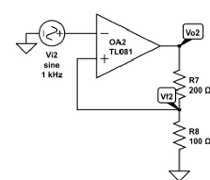
If the input voltage is supplied at a positive pin, then It behaves as a non-inverting op-amp, and the output voltage will be in a phase of the input voltage. On the other hand, if the input voltage is supplied at the negative pin, the output and input voltages will be out of phase and it will behave as an inverting amplifier. The circuit diagrams of both inverting and non-inverting amplifiers are given below:
Non-Inverting Amplifier Example Circuit
Inverting Amplifier Example Circuit
TL081 Applications
The TL081 IC can be used in countless applications. Few of them are listed below:
- Sample and Hold Amplifiers
- It is used in active Filters for amplifying the output signal
- Comparators, Multivibrators, Peak Detectors, square wave oscillators, and function generators also use this IC for designing their internal circuits.
- It can be used to perform all Standard Operational Amplifier Applications as it is pin to pin compatible with the LM741 IC design.
- Operational amplifiers are used in Notch filters for removing a single frequency or a small band of frequencies. Therefore, this IC can also be used for performing this function.
- The IC 7481 is used in applications requiring the summing of voltages like audio mixers.
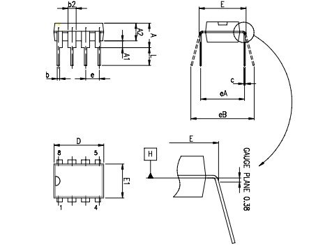
2D Diagram
The TL081 IC is available in 8 pin packages of SOIC and PDSO. Both packages have different dimensions. The two-dimensional diagram of PDSO package is given below:


Hi, your “Inverting Amplifier Example Circuit” is not an amplifier but would make a nice square wave output.