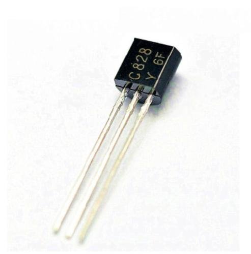
2SC828 is an NPN type silicon epitaxial planar transistor. It is used for switching and signal amplification in audio AF based applications. This transistor is designed for low power applications. Because peak and normal collector dc current is 100mA and 50mA respectively.

2SC828 Pinout
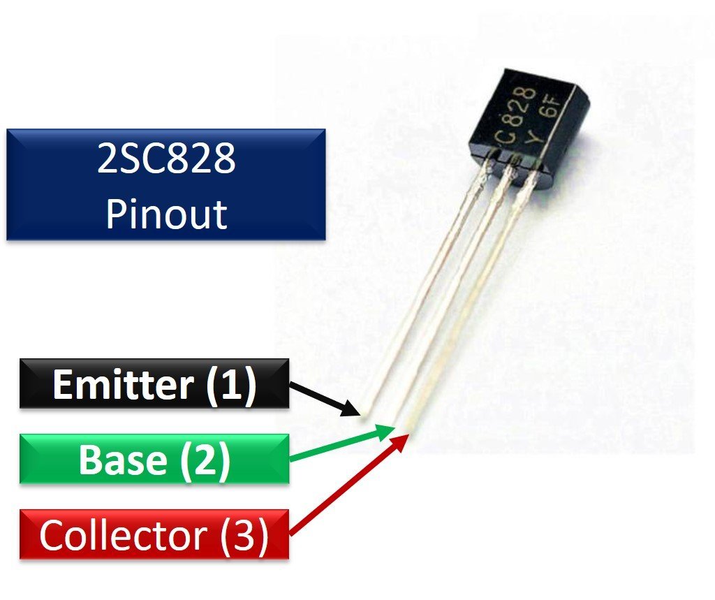
Like other NPN transistors, this silicon epitaxial planar also consists of three pins. By looking at the front end of 2SC828, the leftmost pin is an emitter pin, middle terminal is a base and rightmost terminal is collector pin. The following figure shows the pinout diagram:

Pin Configuration
This table list the pin configuration details:
| Number | Pin Name | Function |
|---|---|---|
| 1 | Emitter | 2SC828 emitter pin |
| 2 | Base | Base pin |
| 3 | Collector | Collector pin |
2SC828 Transistor Features and Specifications
- VCBO (Collector Base Voltage) : 30 Volts
- VCEO (Collector Emitter Voltage) : 25 Volts
- Peak Collector Current : 100mA
- Rated collector current: 50mA
- Power Dissipation: 400mW
- Three different variants according to DC current gain rating (Q, R and S)
- Low side switching for low power application due to NPN type
For more information on dc current gain, breakdown voltage of collector, emitter and base, check the datasheet of 2SC828. The link to the datasheet is given at the end of the article.
Alternative Options
2SC828 Example Circuits
Sine wave generator circuit for flyback transformer testing
In this example circuit, we design a sine wave oscillator circuit from the flyback transformer of a television using one 2SC828 NPN transistor. This circuit consists of three capacitors, two resistors and one variable resistor. It produces a sine wave at the emitter terminal of the transistor. This circuit is a part of a flyback transformer testing circuit.
Low Side Switching Circuit
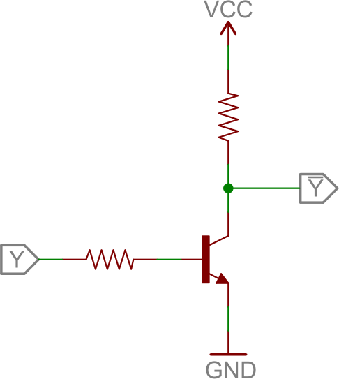
There are two main configurations of transistors when used in switching applications such as low side and high side configuration. In low side switching, the emitter terminal is connected with the ground and the load is connected between the positive terminal of the power supply and collector terminal of the ground. On the contrary, in high side configuration, the load is connected between the collector terminal of the transistor and ground. Usually PNP transistors are used for high side switching and NPN transistors are used for low side switching.

This example circuit shows the use of 2SC828 transistor in low side switching. The 2SC828 NPN transistor acts as a switch to turn on/off load. The control on/off signal is provided to this switching circuit through the base terminal of the transistor. When an active low signal is provided to the base terminal, the transistor does not operate and the connected load will remain off. Similarly, when we apply an active high control signal to the base pin of 2SC828 NPN transistor, it turns on and the switching path of the transistor completes from V+ to ground which turns on the load.
Applications
- Audio frequency amplifier circuits
- Low side and low power switching applications
- Oscillator circuits to produce square wave and sine wave signals
- Amplitude transmitter circuits
2D Diagram
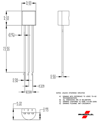
The following figure shows the two dimensional diagram of 2SC898 NPN transistor. The physical dimension diagram electronics components are required while designing a PCB card.

Datasheet
To explore more and to see if this NPN transistor fits into your project according to the output voltage and current requirement, download the datasheet from this link:
Very use full
We needs some PA (Transmitter) VHF & HF transistors for epaire of some old set kindly help Data & availability.