In this tutorial, we will discuss the analog to digital converter. An analog to digital converter (ADC), as its name indicates, is an electronic device that converts continuous time-varying analog signals into discrete-time digital signals so that they can easily be read by the digital devices. It has many applications in electronics projects. ADC converts the physical quantities of a real-world phenomenon into a digital language that is useful in control systems, data computing, data transmission, and information processing. The figure below shows the input/output relationship of an ADC.
Analog to Digital Converter Introduction
Usually, transducers can also convert the input analog variables into currents or voltages. Basically, the digital numbers it uses are binary, i.e., ‘0’ and ‘1’. The ‘0’ indicates the ‘off’ state, and ‘1’ represents the ‘on’ state. Hence, an ADC converts all the analog values into digital binary values. For example, if we have to install an alarm in our house or at some facility whose function is to set off in case of fire or overheating, our whole alarm system will be electronic, but the temperature sensor will give analog values at the output after sensing the temperature. Therefore, to convert the varying values of temperature into digital or discrete values, we have to use an analog to digital converter.
A/D Conversion Process and How ADC works ?
Mainly, there are two steps for the analog to digital conversion:
- S/H: Sampling and holding
- Q/E: Quantizing and Encoding
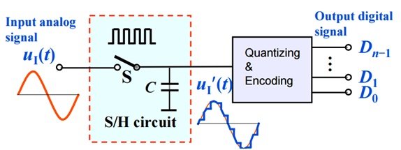
We can see the ADC process in the figure below:
1. Sampling and Holding
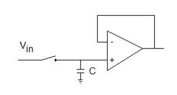
An analog signal continuously changes with time. In order to measure the signal, we have to keep it steady for a short duration so that we can sample it. We could measure the signal repeatedly and very fast and then find out the right time scale, or we could measure the signal at different times and then average it. The last preferable option is that we can hold the signal for a specific duration and then digitize the signal and sample the value. We can do this using a sample and hold circuit. For at least the time required for digitization, it keeps the value stable. The below figure shows the circuit for sampling and holding a signal.
We keep the switch normally open, and when we want to find a measurement, we close the switch momentarily.
2. Quantizing and Encoding
On the output of (S/H), a certain voltage level is present. It assigns a numerical value to it. Then search for the nearest value in correspondence with the amplitude of the sampling and holding signals. And this value cannot be just any value; it should be from a limited set of possible values. It depends on the range of the quantizer, and the range is in a power of 2, i.e.,e 2n (28 = 256, 210=1024 etc.).
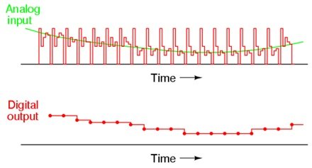
After identifying the closest value, it assigns a numerical value to it, which is encoded in the form of a binary number. The binary-encoded numbers generated by quantizers are represented by ‘n’ bits. The resolution of an ADC can also be denoted by an ‘n’ bit. The figure shows the whole conversion process:
The values we get after the quantization and encoding process cannot be said to be thoroughly accurate. These are only approximations of real-world values. The accuracy of the quantizer highly depends on the resolution of the quantizer; the greater the resolution, the more accurate the values will be. The ADC resolution has limits due to a number of constraints, out of which time is a major issue. If it needs to search for the closest value from a set of possible values and it is greater, then it will surely take more time. But to accelerate this process, more techniques have been developed.
The following table shows the performance of different ‘n’ bit ADCs. If the number of bits is greater, then the frequency is less and the time consumption is also greater. On the other hand, the error minimizes as the number of bits increases. The maximum sampling rates have also been indicated in the table.
ADC Types
The most common types of analog to digital converters available are:
- Flash Analog to Digital converter.
- Dual slope Analog to Digital converter.
- Successive Approximation Analog to Digital Converter.
1. Flash ADC
Flash ADC is one of the simplest ADCs. It is also known as the parallel ADC converter. It consists of a number of comparators. An encoder circuit connects to the output of the comparators, which gives us binary output. The below figure shows a flash ADC circuit of 3-bits:
Vref is the reference voltage; if the analog value at the input becomes greater than the reference voltage, then the comparator output will be high. The flash converter is the most efficient of all the converters in terms of speed. But the number of comparators increases as the number of bits increases. We would require 7 comparators for 3-bits and 15 comparators for 4-bits. This is the disadvantage of using a flash ADC.
But a flash converter can produce a non-linear output, which is an additional advantage. The voltage divider network consists of equal-value resistors, which provide a proportional response. But for special applications, the value of the resistors is changeable, which will give a non-linear response.
2. Dual Slope ADC
A dual-slope integrator first integrates and then disintegrates a voltage signal. It integrates an unknown voltage for a fixed time and disintegrates for a variable time using a reference voltage. We can see the graph of dual slope integration in the figure below.
The main advantage is that the error occurring in a component during integration cancels out during the phase of de-integration. The figure below shows a dual slope converter block diagram:
For example, if we want to obtain a resolution of 10 bits, we would integrate for 210= 1024 cycles and then de-integrate for 1024 cycles. By increasing the number of clock cycles, we can obtain more resolution.
Successive Approximation ADC
This ADC does not count in the binary sequence; its register starts with the most significant bit and finishes at the least significant bit. The comparator’s output is continuously monitored and compared with the analog signal input. This strategy gives much faster results. The figure below shows the workings of this successive approximation register:
The operation of this ADC can be observed in the following graph:
So far, we have discussed the three most common types of analog to digital converters, but there are other converters as well, such as Sigma Delta, digital ramp adc, tracking ADC, etc., which are also widely used converters. You can read this article for an in-depth guide on successive approximations of ADC:
ADC Applications
If we look around, we can notice hundreds to thousands of ADCs and DACs in our daily lives. Some of the popular applications are:
- Audio applications: For example, when listening to music on our mobile phone, the mobile phone stores music in memory in digital form, and a speaker accepts an electrical signal, which is an analog signal. Therefore, we need an ADC to convert a digital bitstream of music into an analog signal to play the music so that we can hear it through a mobile speaker. Hence, our mobile phone contains many ADCs for audio and many other applications.
- Call receiver and transmitter on mobile phone.
- Video Streaming
- Data Acquistion
Conclusion
In conclusion, this tutorial provides an in-depth overview of analog to digital converters. It covers a basic introduction along with working techniques and their types. After this, we discuss the applications of analog to digital converters to help us better understand their usage in our daily lives. You can utilize this based on which suits your project best. Hopefully, this was helpful in expanding your knowledge.
Related Articles:
- Binary Weighted Resistor DAC
- R-2R Ladder DAC
- Introduction to Single Layer PCB – Application and Advantages
- PID Controller Working and Tuning Types
- Fuzzy Logic System: How fuzzy logic control system works?
- Difference Between C and Embedded C Language
Photo Credits:
- successive approximation method by allaboutcircuit
- difference between ADC and analog by allaboutcircuits
This concludes today’s article. If you face any issues or difficulties, let us know in the comment section below.


Why does some ADC and DACs need a externa lpower supply and some dont, What’s the difference?
help me with detailed steps on how to create the lifi internet transmitter and lifi internet receiver and how to configure it to browse on the desktop(implementation at home)
Help with videos and theoretical writs be it using the bread or pcb or empty circuit board
I am sure this piece oof writing has touched all tthe
internet users, its rrally really pleasant paragraph oon building up
new webb site.
I was excited to uncover this website. I need to to thank you for
ones time just for this wonderful read!! I definitely savored every
little bit of it and i also have you book marked to see new stuff in your
website.
Just simply amazing
The provision is very good and it is easy to use> Thank you