In this tutorial, we will talk about successive approximation ADC. This type of ADC converts an analog signal into a digital signal using a binary search through all possible quantization levels. Firstly, we will discuss what ADC is. After that, we will discuss the introduction, working, example circuits, advantages, and disadvantages of successive approximation ADC.
ADC Introduction
ADCs are the bridge between the real world and the digital world. All the information, whether it be temperature, audio, pressure, etc., is in the form of continuous analog signals. But to process and manipulate these signals, we need to interface them with microcontrollers and processors and translate them into their digital representation. This is where analog-to-digital converters come in handy. These are the essential blocks that convert real analog signals from the sensors to binary set values.
How ADC Works?
The ADC is a device to convert analog sine waves to binary digitals for data acquisition. The two key elements that determine the precision of an ADC are the sampling rate, which is based on the Nyquist theorem, and bit resolution, which shows how accurate the output signal is.
Sampling Rate
The input signal samples at the Nyquist rate, which says that the sampling frequency needs to be twice the signal’s frequency of interest. This avoids the aliasing or overlapping of the signals to retain all the information and avoid data distortion or loss. The samples are then assigned finite levels by a process called quantization, followed by the encoding of the signal into binary format.
Quantization Error
It is the difference between the assigned value and the closest available digital value at each sampling point. The formula for the quantization error is as follows:
Quantization Error = Vref / 2N
For example, if the reference voltage is 16 volts and the number of bits is 4, then the quantization error is as follows:
Quantization Error = 16 / 2^4
Quantization Error = 1 Volt
It depicts that any input voltage less than 1 volt is considered to be zero. Any voltage greater than 1 volt will change the ADC output voltage. This introduces quantization errors.
Bit Resolution
The resolution of an ADC is based on the number of bits, which tell us about the number of levels an ADC can produce and quantize the input analog signal. The general formula is:
Resolution = 2N
Where N represents the number of bits. The higher the resolution, the more accurate the resultant signals. For a 4-bit ADC, the resolution will be 16.
Though we can implement ADC using various techniques these days, this article will focus on the successive approximation method.
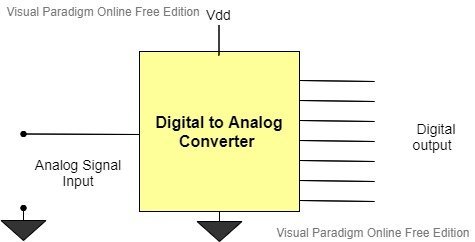
Successive Approximation ADC Introduction
This ADC technique most frequently includes general applications. The ADC comprises a comparator, a digital-to-analog converter, a register, and a control circuit. The schematic is shown below:

At the point when the new conversion begins, the sample and hold circuit samples the input voltage. and then this sampled signal is compared with the output signal of the digital-to-analog converter.
4-bit Successive Approximation ADC Example

To grasp the concept, consider a 4-bit ADC with a sampling rate of 11.2 volts. We take the comparator reference voltage as 16 volts. Whenever the new transformation begins, the successive approximation register sets the most significant bit to 1 and all others to zero. As the register is followed by the DAC, the input to the DAC is 1000. So the output voltage of the DAC corresponding to this digital code and the reference voltage of 16 turn out to be:
Vout = – Vref { B0 (1/16) + B1 (1 /8) + B2 (1/4) + B3(1/2) }
Vout = 8 Volts
This is the threshold voltage to compare with the input voltage. Thus, the output voltage of the comparator will change the output value of the successive registers.
This sets two conditions:

When Vdac < Vin
If the output voltage of the DAC is less than the input voltage, then the most significant bit remains intact, and the next bit will change to 1 for a new comparison.
When Vdac > Vin
On the other hand, if the output DAC voltage is greater than the input voltage, then the MSB is transformed to zero but pulls the next bit high for the new comparison.
Working of Successive Approximation ADC
As per our calculations, the output voltage of DAC is 8 volts, and Vin is 11.2 volts. So, this satisfies the condition Vin>Vdac, which results in no change in the most significant bit, and successive bits are set to 1. Now, the code has become 1100. So, the output of the DAC corresponding to this binary code is 12 volts; we measure it using the same output voltage formula. This is the new DAC voltage to be compared with.

Once more, compare the input voltage with the DAC voltage. If again, the latter is less, then the second bit remains the same while the third bit is made 1 for the new comparison. But if vice versa happens, then the second bit changes to zero and the third bit to 1 for the next comparison. It means that the current input code for the DAC is 1010. We will deduce the output voltage, which is updated to 10 volts. Repeat the same process again.

If Vin is less than 10 volts, then the third bit is kept as it is and sets the least significant bit to high. For vice versa, the third bit turns to 0, and the LSB alters to 1 to compare with the input voltage. The input is for sure greater than the Vdac so the next input code is 1011. The corresponding output voltage becomes 11 volts. It is again compared, and the final code is 1011.

Below is the tree hierarchy that depicts all the possibilities that occur during the iterations. Hence, on the basis of comparison, we only select one code at the end.

Time Domain Representation
The four-cycle time-domain representation of the sequence for the visual is as follows:

Conversion Time
It is the time when an analog-to-digital converter needs to completely convert continuous signals to digital signals. The basis of the conversion time is the number of bits, because the N number of bits takes the N number of clock cycles. Each bit iteration takes one cycle. So, the general conversion time formula is:
Tc = N x Tclk
We can see that the conversion time is independent of the input voltage, which is not the case in the majority of the other ADCs.
Conversion Speed
The speed with which the conversion of the signal takes place is called the conversion speed. Successive Approximation ADC’s typical conversion speed is between 2 and 10 Mega Samples Per Second. (MSPS).
Successive Approximation ADC Resolution
Talking about the resolution, it is the number of bits the analog to digital converter utilizes to discrete the analog inputs. The typical resolution of the successive approximation analog-to-digital converter is in a wide range, starting from 8 bits to 16 bits. Still, some exceptions can resolve up to 20 bits.
SA DAC Latency
Data latency is the time taken by the converter to make the data available for download. It is measured in either time or conversion cycles. If the data is available after a single conversion cycle, then it is called a zero-latency ADC. The successive approximation is a zero-latency ADC. So, it is used in applications where data is required immediately.
Advantages
- They output the binary representation serially.
- They are highly accurate due to their high-resolution.
- Successive Approximation ADCs are reliable and power effective.
Disadvantages
- As the resolution increases, the ADC slows down.
- Its accuracy can drop due to noise and variations in reference voltage.
- It might be unsuitable for applications that require very fine levels of detail.
Applications
| Embedded Systems | Energy Monitoring and Control |
| Medical Instruments | Consumer Electronics |
Conclusion
In conclusion, this tutorial provides an in-depth overview of successive approximation ADC. It covers the basic introduction of ADC, its workings, and moves towards successive approximation ADC. Then we discuss the example along with its workings, advantages, disadvantages, and applications. Hopefully, this was helpful in expanding your knowledge of successive approximation ADC.
You may also like to read:
- ADC STM32F4 Discovery Board
- ADC TM4C123G Tiva C Launchpad
- Display ADC value on 4-digit 7-Segment Display using Pic Microcontroller
- PIC Microcontroller ADC
- HX711 24-Bit Analog-to-Digital Converter (ADC) for Weigh Scales
- ICL7107 ADC Display Driver
- ADC0804 ADC
- ADS1115 I2C external ADC with ESP32 in Arduino IDE
- How to use ADC of ESP32
- How to use ADC of MSP430 microcontroller
This concludes today’s article. If you face any issues or difficulties, let us know in the comment section below.
Approximation ADC – Analog to Digital Converter are used in mobile & wire station ?In Ericssion T18 mobile the chip maybe is N235.
Hello,
I recently working with digital processing data of a piezoelectric sensor vibration and I will integrated with STM32F429I.
How can I can ensure this data
thank you