Altium designer PCB designing tutorial step by step guide: In this article, we will learn how to use Altium designer for PCB designing. I will teach you step by step how to create schematic with Altium designer ? How to create components schmatic symbols with Altium designer? How to make PCB foot prints with Altium designer? And at end I will show you how to design PCB with Altium designer? I have already posted a tutorial on PCB designing with proteus and PCB designing with EasyEDA. But In this article, I will write about Altium designer only. Altium designer is very popular PCB designing software in among industrial people. Due to its expensive price, it is not so much popular among students. But students can still use Altium designer trail version for 30 days. So lets start with Altium designer by seeing how to create your first schematic with Altium designer.
How to make schematic with Altium designer?
Today, I’ll start in this part by making a schematic and in the next part I’ll make a PCB layout for the same schematic. Now to get started,
- I’ll create a new project to work in. I’m in the projects I’ll right-click and add a new PCB project.

- In this project, by right clicking I’ll add a new schematic. Then I’m going to choose add existing project because I’ve got the schematic. As you can see in fig 2.

Now I’ve prepared for schematic and this is schematic that I’m going to work with. So here’s the circuit. I’m going to be recreating. It’s just there as a reference for me and to move around the schematic, you drag it with the right mouse button and to zoom in and out, we can drag with the middle mouse button. And what we see her that we have a couple of resistors, couple of capacitors, a couple of headers and a chip and by making this I hope, I’ll be going through the most basic things which you need to know for making a simple schematic.
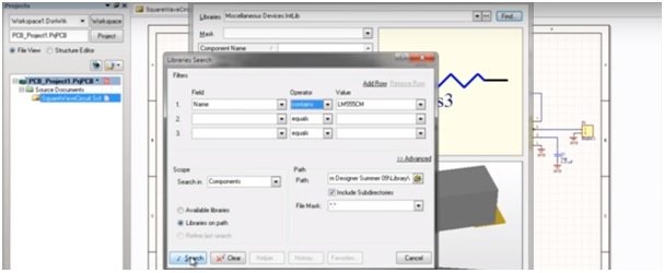
- Here I have quite a few options, I can either use the libraries tab on the left where I can choose the library and look for the components. I could use the place part dialogue which I can bring up either by clicking. By clicking at the place part or by using the keyboard shortcut P. So I’m going to use this for the first And to look through the library, I’m going to click here. As shown in figure 3.

- Here opens a browser so the component I want to start with is that integrated circuit and that doesn’t exist in any of default libraries that are included by default. As shown in fig 4.

- Here I found another part in other libraries, so I’m going to type in it, the name of component. If you are not sure about the name, you can change this to As shown in figure 5.
- And in a search for that usually you would have to make some components yourself. As shown in fig 6.

- And there are already existing some parts in the library. So here’s the part, I want and I can choose a footprint that I want. L M or N means; that’s the standard suffix for showing the pad sizes. N is normal, which is sort of in the middle and you have M which is the most biggest pads and L mean least, which are the smallest pad you can get. Which is good for high-density design and stuff like that I am going to choose the nominal because I am not making anything special and click OK and at next click Yes to install this library. Show in fig 7.
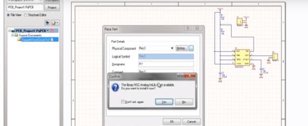
- And next again I click Ok in previous window. Then that part will be generated as in fig 8.

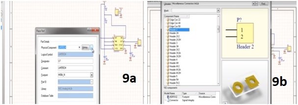
- Going back by right click to previous window (place part dialogue), now right click or you can press the Escape Both of them usually work the same way. Now I found the 3 5 5 5 chip and I am going to look for the resistors, capacitors, and place those as well. Fig 9(a) and I will find headers in the misc connectors library header. Fig 9(b) press ok and again does ok. And make P1 first.
- Then I can click the X or Y to flip it the right way. Fig 10.
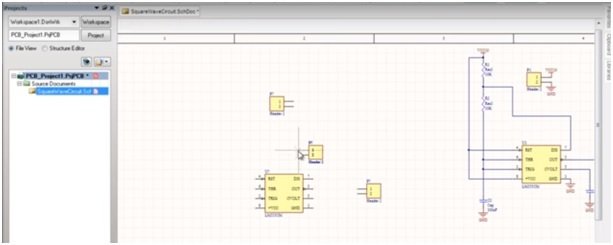
- Now I right click/ press Escape and it just brings me back to the part selection again and for the resistor, those can be found in misc devices and the one I want is the RS3 resistor again press ok like previous, space to rotate and click it to place. Right-click again and now I’m going to click here to find the capacitors again. And those can be found in misc devices. Fig 11.

- After that I place these as before, right-click to cancel that and now finish up by placing the Power Ports. Already we have here 2 types of power ports (VCC10 and GND). Fig 12
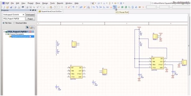
- Text default, here we have VCC and to change that before placing, I can press tab and specify the name that I want for this. Fig 13. Then press Ok

- Now I place VCC10 and you will notice that the Red Cross appears in the junction and that indicates that electrical connection will be made.
- After placing VCC, now we place the grounds and finish off. Now I am going to place wire. Fig 14

- Now I can set the component value. And now double click the value to change it. Then editing it directly. Fig 15. Last option is to specify the value and delete the capacitor and go into the place portal and use the capacitor from here.

- Before placing them, press tab here I specify the value and add the footprint..
- Before I finish I have to give the components unique reference designator names. Fig 16
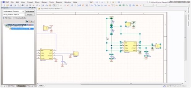
Now all the question marks and names here. So go to a pair on tools and schematics quietly that’ll do it quickly and directly and Save this.
How to design PCB with Altium designer?
In this part, we will make PCB layout for the schematic of altium designer which I did in first part. All the components had unique reference designator. You’ll have to do that to go to PCB layout. Let’s start.
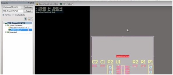
- Add PCB in this project from where we took new project. Now save the PCB file in project directory. Now I can synchronize them.
- Then I go up to an icon named design and import changes. I’ll execute those and those all are successfully in working here so I closed this dialogue.
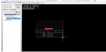
- Just I move around just like you would in the schematic drag with the right button to pane drag with the middle mouse button to zoom in and out. And here see a collection of components. As shown in fig 1. The red rectangle which is a room and we see that this room as the name square wave circuit that corresponds to the schematic sheets named square vase wave circuit. This tells you that rooms are automatically generated for each schematic in your project.
- Now I resize the room and set it at the corner. The entire black area and put here room. Now go up to on design board> board shape> redefine board shape.
- Now I start placing the corners of board place where you can see the edge mode is in 45-degree angle mode. So to toggle between different edge modes or corner much I should say you use shift space just do that a couple of times and you will get a 90-degree corner. As sown in fig 2.
- Now I edit origin and I will set my origin somewhere smart like a corner of your board. Set the layers from design > layer stack manager. Here you can add layers as you wish or plains.
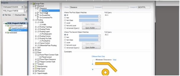
- Now make sure the rules from designs. I can set the rules manually. If you really lazy, you’ll only set the clearance and Trace width. Shown in fig 3. You check them with the specifications that your manufacturer gives you.
- Now I can move components around placing them in the arrangement that seems good for the routing. As sown in fig 4(a). Now join these as you can see in fig 4(b)


- Now that pressing tab gives you a list of a collection of settings that you can specify the trace width but you can also specify how Altium Designer behaves routing.
- You can choose different modes. See fig 5. I recommend turning on push obstacles and turning on follow miles trail and also try Strong You must try different things to see how they work. Well now press OK.

- Now complete its junctions. As you can see in fig 6. Now have got my board wire. Now go to Files> Fabrication outputs> Greber files.

- After choosing Gerber files, I can specify the resolution. Here I can choose the layers that I want to include because this is just one layer board so I choose the first to player copper the top solder mask. Now click
- Now for Drill files, I will go to PCB again. Here on the fabrication outputs and choose NC Drill Files and remaining options leave as default
- Now go to Files and import the Dell files. I would navigate to the project directory and to the projects output directory. After selecting drill files, Click Ok. Now you can see the holes as shown in fig 7
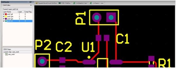
- Now I can close these documents because the Gerber’s and the Drill files are not inside these files. Now just find the Gerber’s for this project. They are located in the project outputs directory. Here I have these three Gerber’s files depending on the number of layers. As shown in fig 8.

- And the Drill files with the extension of .DRL. And that should be enough to get you started should also read the documentation and check your manufacturer.