This tutorial is an introduction to the TM4C123 Tiva C Series LaunchPad from Texas Instruments. We will introduce the TM4C123GH6PMI microcontroller and the development board it ships on, review its key features, then walk through the pinout, GPIO ports, memory map, and on-chip peripherals available on the LaunchPad. Finally, we will look at the integrated development environments (IDEs) you can use to program the board — primarily Keil uVision, Code Composer Studio, and Energia.
Recommended Components
The following components are used in this project or are helpful for getting started with TM4C123 Tiva C LaunchPad development.
| Component | How it’s used in this project | Buy on Amazon |
|---|---|---|
| TM4C123G Tiva C LaunchPad | The development board introduced in this guide. | Check Price |
| Micro USB Cable | Connects the LaunchPad’s onboard ICDI debugger to your PC for programming and power. | Check Price |
As an Amazon Associate we earn from qualifying purchases. Prices and availability are accurate as of the date/time indicated and are subject to change.
What You Will Learn
- What the TM4C123G Tiva C Series LaunchPad is and what makes it different from other ARM Cortex-M4 boards
- Key specifications: 80 MHz Cortex-M4F core, 256 KB Flash, 32 KB SRAM, 2 KB EEPROM, FPU, NVIC, MPU
- Complete pinout — front and back headers — and which GPIO pins map to which port
- Onboard peripherals: UART, I2C, SPI/SSI, USB OTG, CAN, ADC, PWM, GPTM timers, SysTick, μDMA
- The TM4C123GH6PMI memory map: GPIO base addresses for ports A–F via APB and AHB
- Onboard components: ICDI debugger, RGB LED, push buttons, reset switch
- The IDEs you can program it with: Keil uVision, Code Composer Studio, Energia, IAR
If you are new to microcontrollers or ARM in general, start with these foundational tutorials first:
Tiva C Series TM4C123G LaunchPad Introduction
The TM4C123GH6PMI is a high-performance 32-bit ARM Cortex-M4F microcontroller from Texas Instruments, with a broad set of integrated peripherals. The Tiva LaunchPad runs the core at up to 80 MHz, includes a hardware floating-point unit (FPU), and supports tail-chaining to reduce interrupt latency between back-to-back ISRs. The chip integrates a Nested Vectored Interrupt Controller (NVIC) with 8 priority levels, a Memory Protection Unit (MPU) for fault isolation, and exposes both JTAG and SWD (Serial Wire Debug) interfaces for programming and debugging.
TM4C123G LaunchPad Features
Here are the key specifications of the TM4C123G LaunchPad development board:
Microcontroller Core
- Processor: ARM Cortex-M4F (with single-precision hardware FPU)
- Clock speed: Up to 80 MHz
- Flash memory: 256 KB
- SRAM: 32 KB single-cycle
- EEPROM: 2 KB on-chip
- Internal ROM: Pre-loaded with TivaWare peripheral driver library and bootloader
Communication Peripherals
- 8 UART modules with IrDA, 9-bit, and ISO 7816 support
- 4 I2C modules (Standard, Fast, and Fast-Plus modes)
- 4 SSI/SPI modules (also supporting Microwire and TI synchronous serial protocols)
- 1 USB 2.0 OTG/Host/Device with integrated PHY
- 2 CAN 2.0 A/B modules
Analog and Timing
- 2 ADC modules sharing 12 analog input channels, 12-bit resolution, up to 1 MSPS each
- 16 PWM outputs from 2 PWM modules (4 generator blocks and 4 control blocks per module)
- 6 × 32-bit / 6 × 64-bit General Purpose Timer Modules (GPTM)
- 1 × 24-bit SysTick timer
- 2 watchdog timers with separate clock sources
- 2 Quadrature Encoder Inputs (QEI)
General Purpose I/O
- 43 GPIO pins available across ports A through F
- 5 V tolerant inputs on most GPIO pins
- Configurable weak pull-up, pull-down, and open-drain
- Each pin can act as an external edge or level-triggered interrupt source, and can trigger ADC sampling
Power and Operating Conditions
- Operating voltage: 3.3 V (3.0–3.6 V)
- Power supply: USB or external 5 V via the on-board regulator
- Operating temperature range: -40 °C to +85 °C (industrial grade)
Development and Debugging
- On-board ICDI (In-Circuit Debug Interface) — programs and debugs over USB, no external programmer required
- Compatible with Keil uVision, Code Composer Studio (CCS), IAR Embedded Workbench, and the Arduino-compatible Energia IDE
- TI provides the comprehensive TivaWare driver library as a starting point
These features make the TM4C123G LaunchPad a versatile platform for embedded systems development, robotics, motor control, IoT, and learning ARM Cortex-M architecture in general.
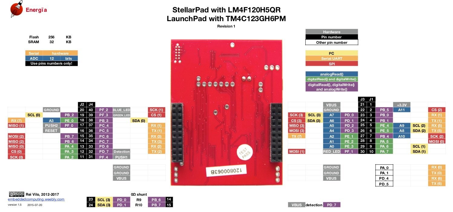
TM4C123G LaunchPad Pinout Diagram
The TM4C123G LaunchPad exposes its GPIO pins through two double-row headers (J1/J2 on one side, J3/J4 on the other). The figure below shows the front-end (top) pinout:
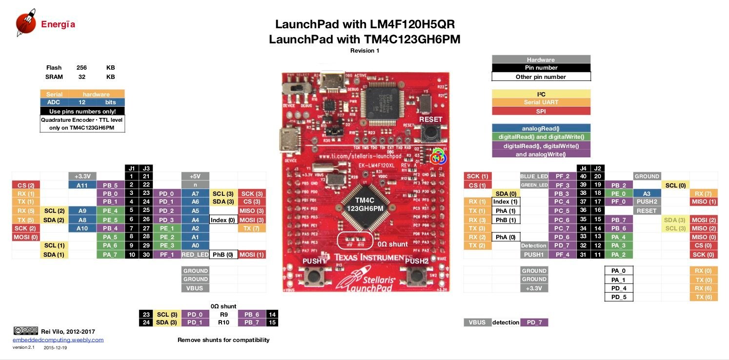
And the back-end (bottom) connector pinout, which exposes additional pins not on the top headers:
TM4C123GH6PMI Microcontroller Features
The TM4C123GH6PMI microcontroller is the actual ARM Cortex-M4F chip on the LaunchPad, running at up to 80 MHz. The clock to each I/O port circuitry can be enabled or disabled individually using the RCGCGPIO register — disabling unused ports saves power, which matters for battery-powered designs.
The diagram below shows how the TM4C123GH6PMI’s pins map internally to the on-board headers and peripherals:
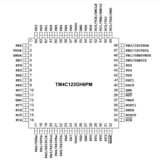
GPIO (General Purpose Input Output)
The TM4C123GH6PMI has 43 general-purpose I/O pins distributed across six ports (A–F). Any GPIO pin can serve as an external edge or level-triggered interrupt source, can trigger ADC sampling, and can toggle at speeds up to the CPU clock when accessed through the AHB (Advanced High-Performance Bus). Most input pins are 5 V tolerant. Every GPIO pin offers configurable weak pull-up, pull-down, and open-drain modes.
Each GPIO port has its own register block at a specific base address in the memory map. The APB (Advanced Peripheral Bus) base addresses for all six ports are listed below:
| Port | APB Base Address | APB End Address |
|---|---|---|
| GPIO Port A | 0x40004000 | 0x40004FFF |
| GPIO Port B | 0x40005000 | 0x40005FFF |
| GPIO Port C | 0x40006000 | 0x40006FFF |
| GPIO Port D | 0x40007000 | 0x40007FFF |
| GPIO Port E | 0x40024000 | 0x40024FFF |
| GPIO Port F | 0x40025000 | 0x40025FFF |
The same six GPIO ports are also accessible through the faster AHB at base addresses 0x40058000 (Port A) through 0x4005D000 (Port F). The AHB allows single-cycle GPIO access (up to 80 MHz toggle rate) compared to APB’s slower two-cycle access — useful for bit-banging protocols or high-speed I/O. Software selects between APB and AHB access via the GPIOHBCTL register.
For a complete guide to memory-mapped I/O on the TM4C123, see:
Most GPIO pins also have alternate functions — they can be reconfigured to serve as UART Tx/Rx, I2C SDA/SCL, SPI MOSI/MISO/SCK, ADC channel inputs, PWM outputs, or timer captures. Only one alternate function can be active on a given pin at a time, but software can switch between them at runtime via the GPIOAFSEL and GPIOPCTL registers.
The pins are organized as PA0–PA7, PB0–PB7, PC0–PC7, PD0–PD7, PE0–PE5, and PF0–PF4, giving 43 usable GPIOs. Note that PC0–PC3 are dedicated to JTAG/SWD by default and reconfiguring them as GPIO requires unlocking the GPIOCR register — locking yourself out of the debugger is easy if you do this incorrectly. PD7 and PF0 also require unlocking before they can be used as GPIO because they default to NMI and the SW2 push-button respectively.
To learn how to actually use the GPIO pins of the TM4C123 in code, check these tutorials:
- How to use GPIO pins of TM4C123G Tiva LaunchPad
- Use Push Button to Control LED with TM4C123G Tiva LaunchPad
- GPIO Interrupts TM4C123 — Edge and Level Triggered
TM4C123G On-Chip Peripherals
Memory
- 256 KB Flash memory — for program code and constant data
- 32 KB single-cycle SRAM — for variables and stack
- Internal ROM pre-loaded with TivaWare driver library, boot loader, IQMath library, and AES tables
- 2 KB on-chip EEPROM — for configuration data that needs to survive power cycles without burning Flash
Serial Communication Peripherals
- USB 2.0 OTG/Host/Device with integrated PHY
- 8 × UART modules with IrDA, 9-bit, and ISO 7816 support
- 4 × I2C modules
- 4 × SPI/SSI modules (Microwire and TI synchronous serial)
- 2 × CAN 2.0 A/B modules
ADC Modules
The TM4C123 has two 12-bit ADC modules sharing 12 analog input channels (AIN0–AIN11). Each ADC module includes 4 sample sequencers that allow different sampling rates, programmable triggers (software, timer, PWM, GPIO, comparator), and hardware averaging. Maximum sample rate is 1 MSPS per ADC. For a complete tutorial on the TM4C123 ADC:
Memory Protection Unit (MPU)
The MPU lets the firmware define memory regions with specific access permissions (read-only, no-access, privileged-only). It triggers a memory management fault when code tries to access a region in a way it shouldn’t — useful for catching pointer bugs early and required for any RTOS that wants to isolate user tasks from kernel memory.
Timers
- 2 watchdog timers with independent clock sources (one runs from system clock, one from PIOSC)
- 1 × 24-bit SysTick timer — perfect for RTOS tick generation or simple delays
- 6 × 32-bit General Purpose Timer Modules (GPTM) — each can also operate as two independent 16-bit timers
- 6 × 64-bit Wide General Purpose Timers — each can also operate as two 32-bit timers
For complete guides on the TM4C123 timer peripherals:
- SysTick Timer (System Timer) TM4C123G ARM Cortex M4 Microcontroller
- SysTick Timer Interrupt Programming TM4C123 ARM Cortex M4
- TM4C123 Timer as a Counter in Input-Edge Count Mode (RPM measurement)
- TM4C123 Timer in Input Edge Time Mode (pulse duration)
- Timer Interrupt TM4C123 — Generate Delay with ISR
PWM Modules
The TM4C123GH6PMI has 2 PWM modules, each with 4 PWM generator blocks and 4 control blocks. Each generator produces two complementary PWM output signals, giving a total of 16 PWM outputs. The PWM modules support dead-band insertion (essential for H-bridge motor drivers), fault input handling, and synchronized timing across generators. For a complete PWM tutorial:
μDMA Controller
The TM4C123 includes a 32-channel micro Direct Memory Access (μDMA) controller. It can move data between memory and peripherals (or peripheral-to-peripheral) without CPU involvement, supports 8-bit, 16-bit, and 32-bit data sizes, and offers two interrupt-enabled priority levels. μDMA is critical for ADC streaming, UART buffering, and any application where the CPU needs to keep doing real work while data shuffles around in the background.
Nested Vectored Interrupt Controller (NVIC)
The NVIC handles all interrupts and exceptions on the Cortex-M4F. The TM4C123 supports 15 system exceptions (like Reset, NMI, HardFault, SVCall, PendSV, SysTick) and up to 78 device-specific interrupts with 8 programmable priority levels. System exceptions always take priority over user-defined IRQs of the same numeric priority, and tail-chaining lets the NVIC switch directly between two pending ISRs without saving and restoring the stack twice. For more detail:
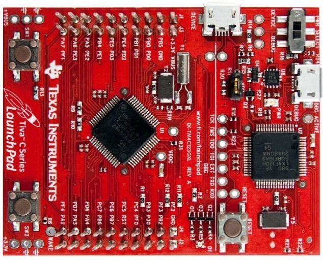
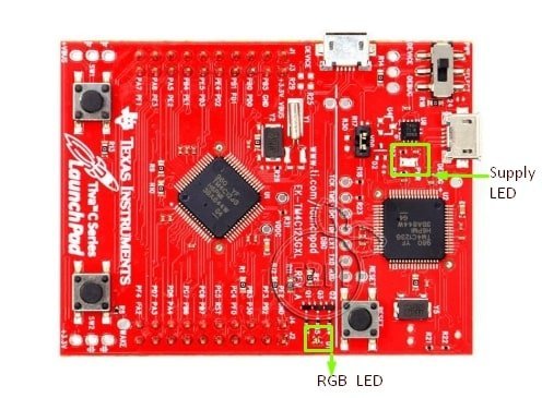
TM4C123G LaunchPad Onboard Components
Onboard Microcontroller and Debugger
The LaunchPad has two main chips visible on the board: the TM4C123GH6PMI target microcontroller (the chip the LaunchPad is named after) and the ICDI debugger chip (a separate microcontroller running TI’s In-Circuit Debug Interface firmware). The ICDI handles JTAG/SWD programming and debugging over USB, and also acts as a USB-to-UART bridge — meaning your sketch’s printf() output appears on a virtual COM port on your PC without any extra hardware.

Push Buttons and Reset Switch
The LaunchPad has two onboard user push buttons (SW1 on PF4, SW2 on PF0), a separate hardware Reset button, and a power source toggle switch (between USB power and external power input). The user push buttons are connected with internal weak pull-ups enabled — they read HIGH when not pressed and LOW when pressed.
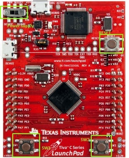
Note that PF0 (SW2) is locked by default — to use it as a regular GPIO input, the firmware must first unlock the GPIOCR register on Port F. This is a common gotcha for first-time TM4C123 users.
Onboard RGB LED
The LaunchPad includes a single tri-color RGB LED wired to three pins of Port F:
- PF1 — Red
- PF2 — Blue
- PF3 — Green
By driving combinations of these pins HIGH (and using PWM for brightness), the firmware can produce any color in the visible spectrum. There is also a separate green power LED that lights when 3.3 V is present on the board.
Datasheet and Reference Documents
The official TI datasheet for the TM4C123GH6PMI ARM Cortex-M4F microcontroller is the definitive reference for register-level programming, electrical characteristics, and detailed timing. You can download it directly from Texas Instruments:
Datasheet link: Download TM4C123GH6PMI Datasheet (PDF)
TM4C123G Block Diagram and Bus Architecture
The TM4C123 uses two on-chip buses to connect the Cortex-M4F core to peripherals: the APB (Advanced Peripheral Bus) and the AHB (Advanced High-Performance Bus). The AHB is much faster — peripheral access takes a single clock cycle on AHB versus a minimum of two cycles on APB. The slower APB is used for low-bandwidth peripherals where speed isn’t critical (UART, basic timers), while AHB is reserved for high-performance modules.
The high-level block diagram of the TM4C123GH6PMI is shown below:
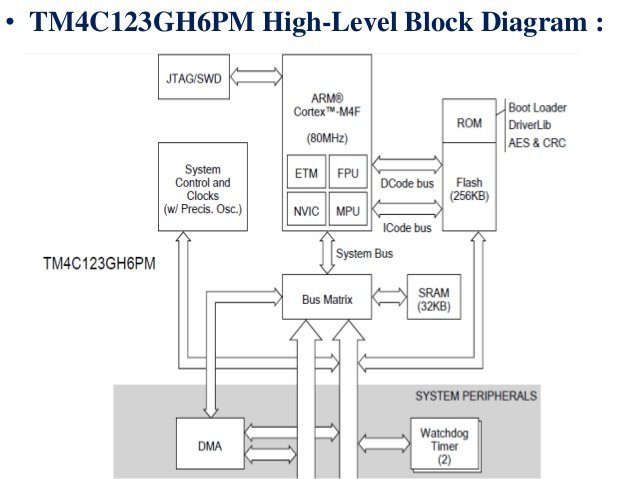
From the block diagram, you can see how the bus matrix routes traffic between the processor core’s I-code, D-code, and System buses to the AHB and APB peripheral buses. Only the GPIO ports and the μDMA controller can be accessed through both AHB and APB — for everything else, the bus is fixed by the peripheral’s design. GPIO is the most common case where you’d want AHB access: high-speed bit-banging or fast register-level toggling.
IDEs for Programming the TM4C123 LaunchPad
You have several options for programming the TM4C123G LaunchPad:
- Keil uVision — popular ARM-focused IDE with built-in debugger and ARM Compiler. Free for code sizes under 32 KB; commercial license needed beyond. This is the IDE used in most tutorials in this series.
- Code Composer Studio (CCS) — Texas Instruments’ free official IDE based on Eclipse. Comes with TivaWare integration and the GCC compiler, no code-size limit.
- Energia IDE — Arduino-compatible IDE for the LaunchPad. Easiest entry point, but hides the register-level details that this series teaches.
- IAR Embedded Workbench — commercial alternative with excellent code optimization, popular in industry.
This tutorial series uses Keil uVision as the primary IDE because it lets you write register-level code directly, which is the best way to actually understand how the Cortex-M4 and TM4C123 peripherals work under the hood. Once you understand the registers, switching to TivaWare in CCS or Energia’s higher-level API is trivial — but the reverse is not true.
To get started with Keil and the TM4C123, follow these tutorials in order:
- How to Download and Install Keil uVision
- Getting Started with Keil uVision: Write Your First Program
- How to Use GPIO Pins of TM4C123G Tiva LaunchPad
- Controlling LED with Push Button using Tiva LaunchPad
- Bare Metal Embedded Systems Linker Script File
- What is a Microcontroller Startup File — Functions Explained
- Microcontroller Booting Process — Reset Sequence
Conclusion
The TM4C123 Tiva C Series LaunchPad is a strong choice for learning ARM Cortex-M4 development — it has a powerful 80 MHz core with FPU, generous on-chip Flash and SRAM, a deep peripheral set (UART, I2C, SPI, USB, CAN, ADC, PWM, multiple timer modules), an integrated debugger, and works with all major ARM IDEs including the free Code Composer Studio. The combination of the TivaWare driver library, well-documented hardware, and the TM4C123GH6PMI’s Cortex-M4F core also makes it an excellent platform for understanding ARM architecture concepts (NVIC, MPU, μDMA, AHB/APB) that translate directly to STM32, NXP, Microchip SAM, and other Cortex-M devices. The next tutorials in this series walk through setting up Keil uVision and writing your first programs for the LaunchPad — start there to begin programming the board.
HI ,
I am new to tivaware series controllers , I would like to enable 8 interrupt in same GPIO port (example PORTA ).Is this possible in TM4C123GXL controller??
Rani L.,
You can enable/disable an interrupt for each individual pin,
You can assign relative priority
You have one interrupt handler per port (at least, for the Texas Instruments’ MSP series, couldn’t tell for sure for this particular Texas Instruments’ MCU. And in this handler, you can identify which pin (of the port, a port having generally 8 pins ) has a pending call (due to priority, they are automatically “stacked” by the NVIC )
Hi,
I need some help working with the watchdog timer (WDT) on the TM4C123 Tiva C series lauchpad. Can you please make a quick tutorial on how to configure and use it?
Thanks!