In this tutorial, we will give an explanatory introduction of a TM4C123G microcontroller namely TIVA C series TM4C123G by Texas instrumentals. We will first give a detailed introduction of the microcontroller used for this development board. After that Pinout, GPIO pins, memory, and different peripherals available on the LaunchPad will be explained. It will include the description of features of every port including GPIO pins. In the end, we will see the different types of integrated development environments (IDE) that are available to program the TM4C123G development board.
If you can just a beginner in microcontrollers programming, you can read these tutorials:
Tiva C Series TM4C123G LaunchPad Introduction
The TM4C123G is a member of the class of high performance 32 bit ARM cortex M4 microcontroller with a broad set of peripherals developed by Texas Instrumentals. The TIVA launchpad has a built-in processor clock frequency of up to 80MHz with a floating-point unit (FPU). The Cortex-M4F processor also supports the tail chaining functionality. It also includes a nested vector interrupt controller (NVIC). The debugging interface used is JTAG and SWD (serial wire debugger) for programming and debugging purposes.
TM4C123G LaunchPad Features
The TM4C123G has a vast variety of applications. It hosts a variety of communication peripherals which can be used to connect all sorts of electronics devices; both sensors and actuators for example IR sensors, motors etc.The TM4C123G is basically a Thumb216/32 bit code that is 26% memory and 25% faster than 32-bit and has a flexible clocking system and can also access real time clock through hibernation module.
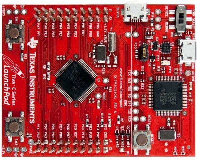
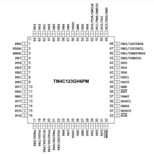
TM4C123G LaunchPad Pinout Diagram
This figure shows the front end pinout diagram:
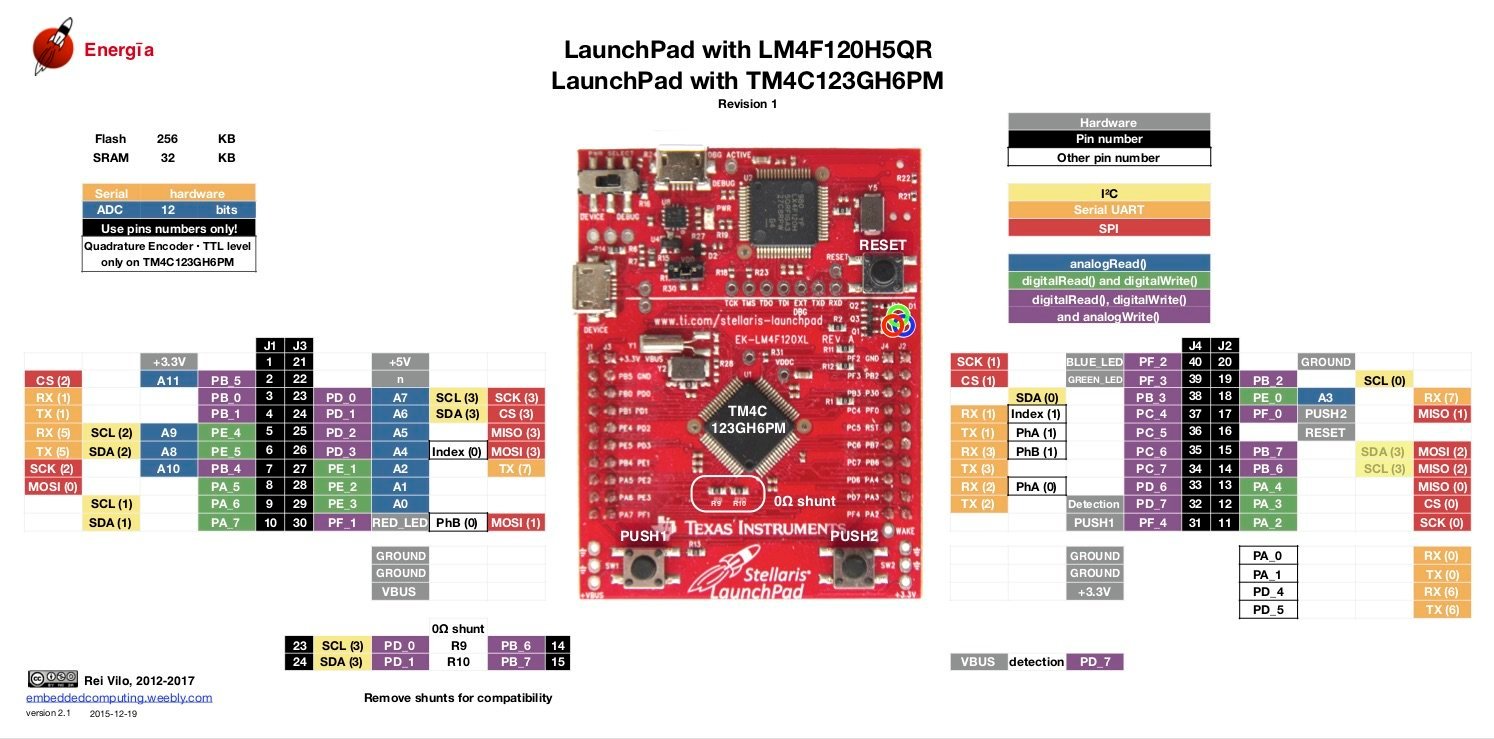
This figure shows the pin confiuration for back end connetor:
TM4C123GH6PMI Microcontroller Features
The TM4C123GH6PMI microcontroller of ARM Cortex-M4F operates at 80MHz clock frequency. The clocked source of the I/O port circuitry of the TIVA board can be enabled using the RCGCGPIO register. The clock source of a pin should be disabled if an I/O port is not used to save power.
The pins of the microcontroller as visible from the above figure are internally connected to the output on board ports and the functionality of the pins of the controller is shown in the figure below:
GPIO (General Purpose Input Output)
It has 0-43 general purpose input-output pins. Any GPIO can be used as an external edge or level triggered interrupt, it can initial ADC sampling, can change toggle rate up to CPU clock speed on the advanced high-performance bus. Each input pin has a tolerance voltage of 5V in the input configuration. Every GPIO pin also has a weak pull-up, pull-down, and open drain.
There are many registers associated with each of the above I/O ports and they have designated addresses in the memory map. The above addresses are the Base addresses meaning that within that base address we have the registers associated with that port.
| Port name | Lower address | Upper address |
| GPIO port A | 0x40004000 | 0x40004FFF |
| GPIO port B | 0x40005000 | 0x40005FFF |
| GPIO port C | 0x40006000 | 0x40006FFF |
| GPIO port D | 0x40007000 | 0x40007FFF |
| GPIO port E | 0x40024000 | 0x40024FFF |
| GPIO port F | 0x40025000 | 0x40025FFF |
In order to understand memory mapped IO, read this tutorial:
Accessing Memory Mapped Peripherals Registers of Microcontrollers
Most of the GPIO pins in a microcontroller can be configured for an alternate hardware function. It should be noted that only 1 of the alternate functions can be configured at a given time. The user program can switch among different alternate functionality during execution.
The general-purpose I/O pins are named as port A to port F in TM4C123G microcontroller. The address range of the GPIO pins are given in the table below,
Port name Lower address Upper address.
These ports are designated as PA0-PA7, PB0-PB7, PC0-PC7, PD0-PD7, PE0-PE5, and PF0-PF4. The figure below shows the onboard GPIO pins of TIVA.
To learn how to use GPIO pins of TM4C123, check these tutorials:
- How to use GPIO pins of TM4C123G Tiva launchPad
- Use Push Button to Control LED with TM4C123G Tiva LaunchPad
- GPIO Interrupts TM4C123
TM4C123G Peripherals and Modules
Memory
It has
• 256 kb Flash memory.
• 32 kb single-cycle SRAM with internal ROM loaded with TivaWare software.
• 2 kb EEPROM which is fast and saves board space
Serial Communication Modules
It also has onboard mounted
- USB 2.0 (OTG / HOST / Device)
- 8 UART ports with IrDA, 9-bit, and ISO7816 port
- 6 I2C
- 4 SPI microwire or TI synchronous serial interface
- 2 CAN Modules
ADC Modules
TM4C123 Tiva C series Launchpad microcontroller has two ADC modules that share 12 analog input channels. On top of that four Sample sequencers are also available as a part of each ADC module to provide different samplig rate, sampling averaging features. In depth guide on TM4C123GH6PM microcontroller ADC modules are available in this article:
Memory protection unit
It has a built-in feature of generating a memory management fault on incorrect access to region.
Timers
It has
- 2 watchdog timers with separate clocks
- 1 SysTick timer, with 24-bit high-speed RTOS and another timer
- Six 32bit and six 64 bit general-purpose timers.
A complete in-depeth guides on systick timer are available on these links:
- SysTick Timer (System Timer) TM4C123G ARM Cortex M4 Microcontroller
- Systick Timer Interrupt Programming TM4C123 ARM Cortex M4
- TM4C123 Timer as a Counter in Input-Edge Count Mode
- TM4C123 Timer in Input Edge Time Mode
- Timer Interrupt TM4C123
PWM Modules
TM4C123GH6PM microcontroller contains two PWM modules and each PWM modules consists of 4 generator blocks and 4 control blocks. Furthermore, each PWM generator provides two PWM output signals. Hence, we can get total 16 PWM signals from TM4C123 Tiva Launchpad. Check this in-depth guide on TM4C123 PWM:
32 Channel DMA
It also has two interrupt enabled priority levels and 8, 16 and 32 bit data sizes.
Nested Vector Interrupt controller (NVIC)
The built-in nested vector interrupt controller is a vector or stack you can say which contains 7 exceptions (defined by the programmer) and 71 interrupts (to be defined by the user) with 8 programmable priority levels. These priority levels decide the priority of the interrupts defined by the user and always have lower priority than the programmer-defined exceptions. Further information on NVIC is available in this article:
TM4C123G LaunchPad Components
OnBoard Microcontroller
Two onboard chips present on the board are debugger and the microcontroller. The debugger mounted on the board is JTAG or SWD as we will see shortly, and the microcontroller chip mounted on the board is TM4C123G after which the board is named. Refer to the figure below:

Push Buttons
There are two onboard switches (Push button) on the LaunchPad that are connected internally with the GPIO pins, and a toggle switch that is used as a power switch, and another push button that is used to reset or restart the program execution that is already loaded on the board. As shown in the figure below:
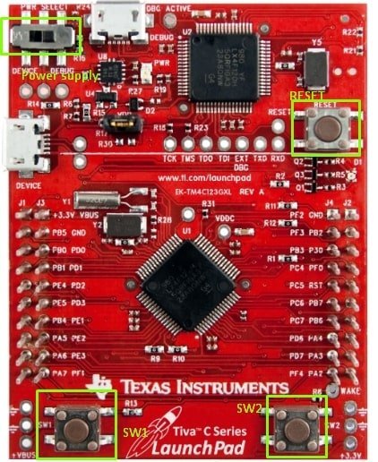
SW1 push-button switch is connected to the PF0 GPIO pin and the SW2 push-button switch is connected to the PF4 GPIO pin.
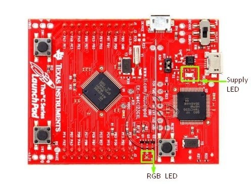
Onboard LEDs
One onboard tri-color LED is also present on the TIVA launchpad which is internally connected to the F port of the GPIO pins, and when enabled the led shows the color of the enabled pin. And also there is a power LED of color green on the board which when on tells the user that the board is turned on. Both the LEDs are highlighted in the figure below.
Data sheets
The datasheet of TIVA TM4C123G ARM-based cortex-M4F microcontroller is available online and you can easily access it through the link given below:
Datasheet link: Download
TM4C123G Block diagram
The ARM chips have two buses: APB (Advanced Peripheral Bus) and AHB (Advanced High-Performance Bus). The AHB bus is much faster than APB. The AHB allows one clock cycle access to the peripherals. The APB is slower and its access time is minimum of 2 clock cycles.
A high-level block diagram of TM4C123G microcontroller is shown in the figure below.
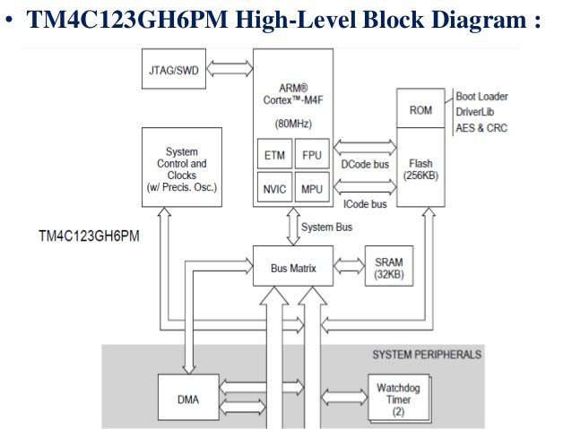
From the figure, it is visible that there are 2 on-chip buses AHB and APB, which connect the processor core to the peripherals. These buses are constructed from the system bus using a bus matrix. It should be recalled that this bus matrix is different from the one used inside the processor block. The bus matrix inside the processor block is responsible for connecting the instruction and data buses from the processor core I code D code to system buses.
The advanced peripheral bus (APB) is the low speed bus. The more complex Advanced High-performance Bus (AHB) gives improved performance than the APB bus and should be used for interfacing those peripherals, which require faster data transfer speed. The block diagram also shows different peripherals modules connected to these two buses. It should be noted that only the GPIO and direct memory access (DMA) modules have connectivity available to both buses.
IDE for programming
There are many options available to write programs for TM4C123G launchpad such as Energia IDE, code composer studio, and Keil. The IDE that we will use for programming the TM4C123G is Keil. It allows you to build a programming interface in the language of your desire. You can write a code to be burnt on the microcontroller in the language of your desire as we will see shortly in the upcoming tutorials.
Check these getting started tutorials for Keil IDE:
- How to download and install Keil uVision
- Getting started with Keil uVision: write your first program
- How to use GPIO pins of TM4C123G Tiva launchPad
- Controlling LED with push-button using Tiva LaunchPad
- Bare Metal Embedded Systems Linker Script File
- What is Microcontrollers startup file – Understand its various Functions
- Microcontroller Booting Process – Reset Sequence
HI ,
I am new to tivaware series controllers , I would like to enable 8 interrupt in same GPIO port (example PORTA ).Is this possible in TM4C123GXL controller??
Rani L.,
You can enable/disable an interrupt for each individual pin,
You can assign relative priority
You have one interrupt handler per port (at least, for the Texas Instruments’ MSP series, couldn’t tell for sure for this particular Texas Instruments’ MCU. And in this handler, you can identify which pin (of the port, a port having generally 8 pins ) has a pending call (due to priority, they are automatically “stacked” by the NVIC )
Hi,
I need some help working with the watchdog timer (WDT) on the TM4C123 Tiva C series lauchpad. Can you please make a quick tutorial on how to configure and use it?
Thanks!