Multiplexers are essential components in digital logic circuits that enable the selection and routing of multiple input lines to a common output line. In this tutorial, we will explore the process of building a 4×1 multiplexer using LabView, a powerful graphical programming language commonly used in data acquisition and instrument control. We will delve into the purpose and functionality of a multiplexer, step-by-step instructions for designing a Virtual Instrument (VI) in LabView, and how to dynamically route inputs to the output based on a selector switch. By following along and engaging in hands-on exercises, you will gain a solid understanding of multiplexer design principles and be well-equipped to tackle more complex circuits in the future. So let’s dive in and unlock the world of multiplexers with LabView!
What is a Multiplexer?
A multiplexer is an essential component in digital logic circuits that enables the selection and routing of multiple input lines to a common output line. It is used to control the flow of data by selecting one input line and directing it to the output line based on the control signals provided. In simpler terms, a multiplexer acts as a data selector, allowing a single output to represent one of several inputs based on a specified condition or logic. The selected input is then transmitted to the output line, while the non-selected inputs are disregarded. Multiplexers are commonly used in various applications, such as data acquisition, signal routing, and memory addressing, to efficiently manage and process digital signals.
A 4-to-1 multiplexer will select one value from the 4 input values depending upon the value given to the selector switches and will display the selected input to the output. At the end of the tutorial you are provided with an exercise to do by yourself, and in the next tutorials I will assume that you have done those exercises and I will not explain the concept regarding them.
4×1 multiplexer design in Labview
Now let’s design a VI performing the operation described above. First of all, create a VI as we have done in tutorial 1 and save it for future use as we have been doing in the entire previous tutorial. From the control palette select Boolean and then select the push button as shown in the figure below:

This push button will be used as a control to give the input to the multiplexer. As we are designing 4×1 multiplexer, the number of inputs will be 4 and hence the number of controls needed. Place 4 similar push buttons on the front panel and name them as I0, I1, I2, I3 as shown in the figure below:

To differentiate the selector switch controls from the input controls, we will use toggle switch instead of push button for selector switches. From the control palette on the front panel select Boolean and then select Toggle switch as shown in the figure below:

Place two such toggle switches for two selector switches and label them properly as shown in the figure below:

As a 4×1 multiplexer uses a multi-input AND gate and a multi-input (more than 2) OR gate and LabView does not have more than 2 input gates, we will use a block named Compound that will be used as a multi-input AND and OR gate. On the block diagram panel, click right and from the function palette select Boolean and then select Compound arithmetic as shown in the figure below:

Place four compound blocks next to the four input controls as shown in the figure below:

In order to change the mode of the compound block to AND, right click on the block and select Change mode and then select AND as shown in the figure below:

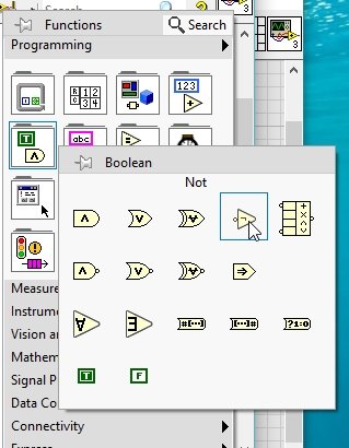
This multiplexer will need the input from the selector switches as it is and also the NOT version of the input from the selector switches. Therefore, we will need a NOT gate also to perform the NOT operation required. From the function palette select Boolean and then select NOT as shown in the figure below:
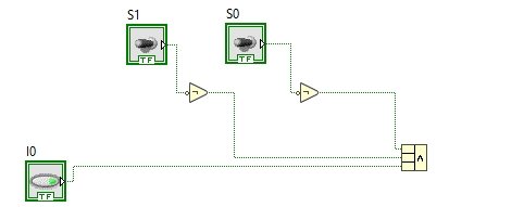
Connect the NOT gate to the selector switches as shown in the figure below:

Now, at the input of the 1st AND (compound) block connect the NOT S0 wire, NOT S1 wire, and the input from I0 as shown in the figure below:
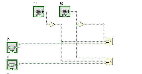
At the input of the 2nd AND (compound) block connect the S0 wire, NOT S1 wire, and the input from I1 as shown in the figure below:
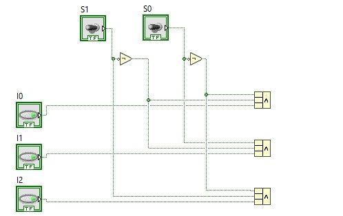
At the input of the 3rd AND (compound) block connect the NOT S0 wire, S1 wire, and the input from I2 as shown in the figure below:
At the input of the 4th AND (compound) block connect the S0 wire, S1 wire, and the input from I3 as shown in the figure below:

Now, to OR the output of all the AND gates, we will need a four-input OR gate, which is not present in LabView. For this purpose, we will again use the compound block and change its mode to OR as shown in the figure below:
At the input of this block connect the outputs from the four AND gate blocks and at the output of it create an indicator as shown in the figure below:

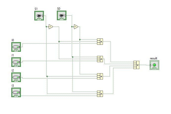
The complete block diagram of a 4×1 multiplexer is shown in the figure below:
Run the VI by using the run arrow or by pressing <Ctrl+R>. The output is shown in the figure below:

Now set the value of the selector switch to 10 in binary, which is equal to 3 in decimal numbers, and the value at the 3rd input (I2) will be transferred to the output as shown in the figure below:

Exercise
- Evaluate the remaining states of the 4×1 multiplexer.
Design a VI that will undergo the operation done by an 8×1 multiplexer.
Conclusion
In conclusion, this tutorial has guided you through the process of building a 4×1 multiplexer using LabView. We have learned about the purpose and functionality of a multiplexer, as well as how to design a VI to dynamically route one of the input lines to the output based on the selector switch. By following the step-by-step instructions and using various components such as push buttons, toggle switches, compound blocks, and NOT gates, we have successfully created a complete block diagram for the multiplexer. Moreover, we have seen how to run the VI and observed the output based on different selector switch settings. This tutorial has provided a solid foundation for understanding the concept of multiplexers and can serve as a starting point for more complex multiplexer designs. By completing the exercise and exploring the design of an 8×1 multiplexer, you can further enhance your understanding of this essential component in digital logic circuits.