2SC1345 NPN transistor is a Chinese, low-noise, and low-frequency transistor, used in audio amplification applications. It is an NPN transistor with an emitter to collector voltage of 50V and the collector current of 100mA. This NPN transistor finds its usage in switching and amplification but it is recommended to not use it as a switch due to its high collector-emitter voltage(50V) ratings and comparatively low collector current(100mA). Furthermore, it has a high gain value ranging from 250 to 1200 making it a perfect choice for low amplification systems.
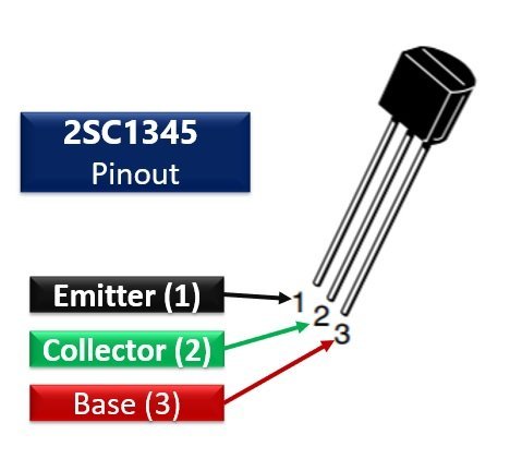
2SC1345 Pinout
This NPN Low-noise epitaxial silicon transistor has three pins conventionally. The leftmost pin is the emitter terminal which supplies the majority of charges and current drains out through emitter terminal. The next pin is the collector pin (center) which is slightly larger than the emitter to collect most of the charges from the emitter. Usually, we connect a load to the collector pin. The rightmost pin serves as the transistor base, which controls the current flow from the emitter to a collector by providing the required biasing voltage to the base terminal.
Following diagram shows the pinout of the 2SC1345 NPN Amplifier Transistor:
Pin Configuration
The pin configuration detail in tabular is mentioned below:
| Number | Pin Name | Function |
|---|---|---|
| 1 | Emitter | Emitter pin |
| 2 | Collector | Collector pin |
| 3 | Base | Base pin |
2SC1345 Features and Specifications
- Collector-Emitter voltage(VCEO) : 50 Volts
- Collector-Base voltage(VCBO) : 55 Volts
- Emitter-Base voltage(VEBO) : 5.0 Volts
- Continuous Collector Current (IC) : 100 mA
- DC Current Gain (VCE=12.0 Volts,IC=2 mA) : 250-1200
This transistor also has three variations based on DC gain described under :
| Part Number | DC Gain(hFE) |
|---|---|
| 2SC1345D | 250-500 |
| 2SC1345E | 400-800 |
| 2SC1345F | 600-1200 |
To check small-signal and noise characteristics, the link to the 2SC1345 datasheet is provided at the bottom of the article.
2SC1345 Alternative Options
- KSC1845FTA
- 2SC2240
2SC1345 Example Circuit
In this section, we will see an example circuits of 2SC1345 as an amplifier :
2SC1345 as a Low-Frequency Amplifier
The diagram shows the schematic of a 2SC1345 low-frequency Amplifier :
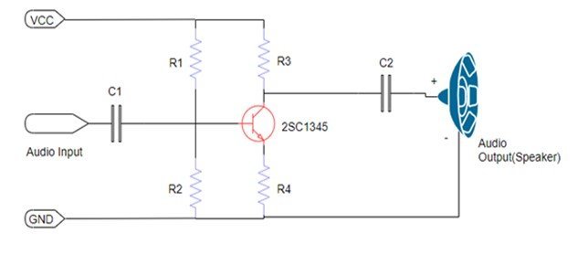
2SC1345 works similarly to other amplifier transistors except for the fact that it is operating at low frequencies. The base terminal is connected with an input signal, and the collector is given input voltage to turn on the active mode and operate the transistor as an amplifier. The resistors are responsible to control the gain by managing the flow of the current Coupling capacitors are used to avoid the distortion of the signals and to control the gain of the amplifier as per requirement. The frequency response of the circuitry is also dependent on these capacitors.
As a low-band frequency input signal is given to an amplification system, the signal reaches the base of the transistor, gets boosted, and is returned in the form of a high gain signal. In the case of an audio signal, it outputs a high sound with fine quality.
APPLICATIONS
- Oscillator circuits
- Modulation of signals
- Low noise amplification systems
- Low power AF systems
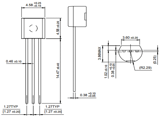
2D Diagram
The following figure shows the 2d model of T0-92(1) package 2SC1345 NPN Amplifier Transistor. It shows us the physical dimensions of the components needed when a PCB card is designed.
DATASHEET
The link to the datasheet is given below to see more details and specifications of the 2SC135 Low-Frequency NPN Amplifier Transistor.
“The leftmost pin is the emitter terminal which supplies the majority of charges and current drains out through emitter terminal. The next pin is the collector pin which is slightly larger than the emitter to collect most of the charges from the emitter. Usually, we connect a load to the collector pin. ***The center pin *** serves as the transistor base (…)”.
[ I added the * ].
It is a typo, since the base pin is the rightmost one, the center pin being the emitter, as mentionned in the text.
You are right. Correction made. Thanks