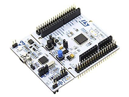
STM32 Nucleo F401RE is a low cost and quick to use a development board. It has an ARM Cortex 32 Bit microcontroller that comes only in a single package LQFP. In STM32 Nucleo there are two types of connection pins. One is used for STM which are male pins and the second are female pins used for Arduino. All types of Arduino headers can be attached to the board. STM32 boards give all kinds of modern communication and debug systems for industrial and home-based with 84MHz procession speed. At the commercial level, the board builds an excellent reputation within a few decades and increases daily.
Pin Configuration of STM32 Nucleo
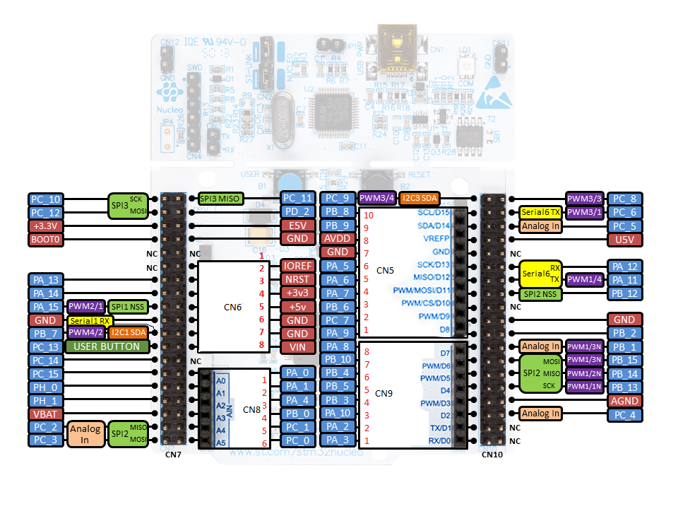
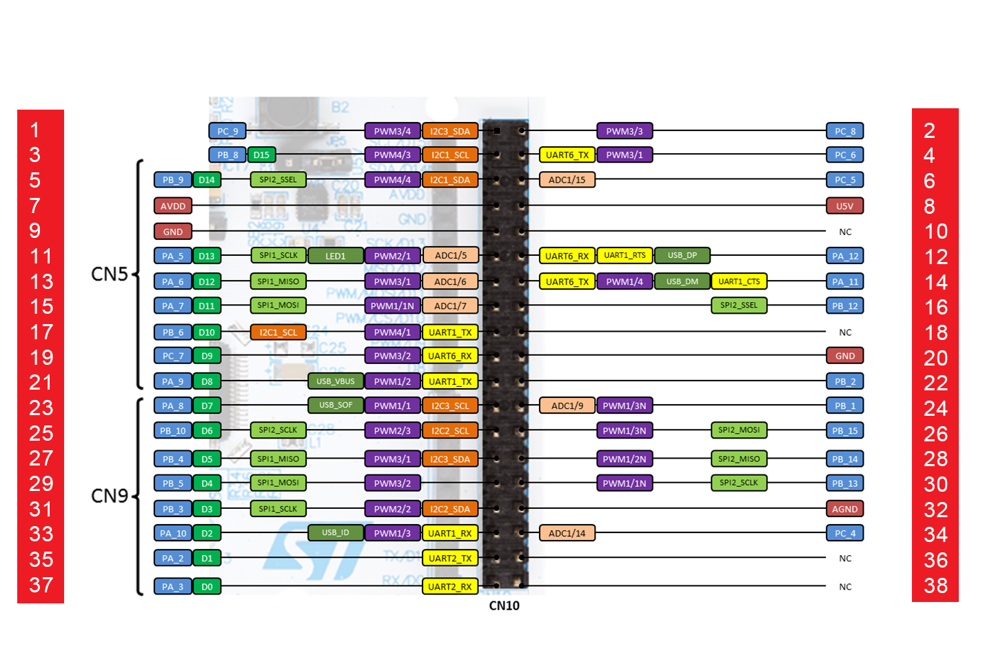
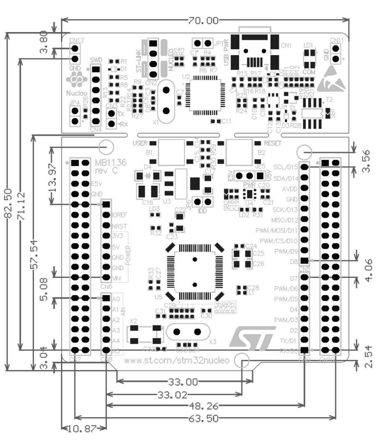
The pin configuration of STM Nucleo is a little different from other boards. It supports the multiple IDE but it has pins for STM32 and Arduino separately. The male ones are for STM32 and females are for Arduino. The female pins can be attached to any Arduino supported shield or module without using any third device. The header CN5, CN6, CN8, and CN9 are for Arduino and C7, C10 represents STM32 Nucleo.
STM32 Nucleo Digital Input/Output Pins
I/O pins are the basic requirement for every circuit. In STM32 Nucleo there are a bunch of them. Some came from Arduino pins and some come from STM32 pin. The I/O pins are lower in number as compare to STM32. Here all the I/O pins of STM32 Nucleo are:
In C7:
- PC10 – GPIO1
- PC11 – GPIO2
- PC12 – GPIO3
- PD2 – GPIO4
- PA13 – GPIO13
- PA14 – GPIO15
- PA15 – GPIO17
- PC13 – GPIO23
- PC14 – GPIO25
- PC15 – GPIO27
- PA0 – GPIO28
- PH0 – GPIO29
- PA1 – GPIO30
- PH1 – GPIO31
- PA4 – GPIO32
- PB0 – GPIO34
- PC2 – GPIO35
- PC1 – GPIO36
- PC3 – GPIO37
- PC0 – GPIO38
IN CN10:
- PC9 – GPIO1
- PC8 – GPIO2
- PB8 – GPIO3
- PC6 – GPIO4
- PB9 – GPIO5
- PC5 – GPIO6
- PA5 – GPIO11
- PA12 – GPIO12
- PA6 – GPIO13
- PA11 – GPIO14
- PA7 – GPIO15
- PB6 – GPIO17
- PC7 – GPIO19
- PA9 – GPIO21
- PB2 – GPIO22
- PA8 – GPIO23
- PB1 – GPIO24
- PB10 – GPIO25
- PB15 – GPIO26
- PB4 – GPIO27
- PB14 – GPIO28
- PB5 – GPIO29
- PB13 – GPIO30
- PB3 – GPIO31
- PA10 – GPIO33
- PC4 – GPIO34
- PA2 – GPIO32
- PA3 – GPIO37
In CN5:
- D0 – GPIO1
- D1 – GPIO2
- D2 – GPIO3
- D3 – GPIO4
- D4 – GPIO5
- D5 – GPIO6
- D6 – GPIO7
- D7 – GPIO8
In CN6:
- D8 – GPIO1
- D9 – GPIO2
- D10 – GPIO3
- D11 – GPIO4
- D12 – GPIO5
- D13 – GPIO6
- D14 – GPIO9
- D15 – GPIO10

PWM Pins
The Nucleo F401RE has multiple PWM pins. PWM pins are available in both STM32 and Arduino. All PWM pins can generate the desired output signal to control the external peripherals. These PWM pins use a Prescaler to break the single cycle of the clock pulse to generate the output signal. All PWM pins are:
In CN7:
- PWM2/1 – GPIO17
- PWM4/2 – GPIO19
- PWM2/1 – GPIO28
- PWM2/2 – GPIO30
- PWM1/2N – GPIO34
In CN10:
- PWM3/4 – GPIO1
- PWM3/3 – GPIO2
- PWM4/3 – GPIO3
- PWM3/1 – GPIO4
- PWM4/4 – GPIO5
- PWM2/1 – GPIO11
- PWM3/1 – GPIO13
- PWM1/4 – GPIO14
- PWM1/1N – GPIO15
- PWM4/1 – GPIO17
- PWM3/2 – GPIO19
- PWM1/2 – GPIO21
- PWM1/1 – GPIO23
- PWM1/3N – GPIO24
- PWM2/3 – GPIO25
- PWM1/3N – GPIO26
- PWM3/1 – GPIO27
- PWM1/2N – GPIO28
- PWM3/2 – GPIO29
- PWM1/1N – GPIO30
- PWM2/2 – GPIO31
- PWM1/3 – GPIO33
IN CN5 & CN9:
- D3 – GPIO5
- D5 – GPIO6
- D6 – GPIO7
- D9 – GPIO10
- D10 – GPIO11
- D11 – GPIO12
Serial Communications in STM32 Nucleo F401RE
UART Communication Pins
There are multiple UART communication pins in the Nucleo F401RE. All these pins allow the multiple UART module to communicate with the board at a time. The UART on Arduino only allows communicating a single UART device. All UART pin in the board are:
In CN7:
- UART1_RX – GPIO21
- UART2_CTS – GPIO28
- UART2_RTS – GPIO30
In CN10:
- UART6_TX – GPIO4
- UART6_RX/UART_RTS – GPIO12
- UART_TX/UART1_CTS – GPIO14
- UART1_TX – GPIO17
- UART6_RX – GPIO19
- UART1_TX – GPIO21
- UART1_RX – GPIO33
- UART2_TX – GPIO35
- UART2_RX – GPIO37
In CN9:
- RX – GPIO1
- TX – GPIO2
SPI Communication Pins
SPI protocols are also a kind of serial communication that uses four-wire for communication. Two for clock and device selection and two for data. Multiple devices of the same kind can be controlled by a single SPI module. In Nucleo F401RE has multiple SPI pins which are:
In CN7:
- SPI3_SCLK – GPIO1
- SPI3_MISO – GPIO2
- SPI3_MOSI – GPIO3
- SPI1_SSEL – GPIO17
- SPI1_SSEL – GPIO32
- SPI2_MISO – GPIO35
- SPI2_MOSI – GPIO37
In CN10:
- SPI2_SSEL – GPIO5
- SPI1_SCLK – GPIO11
- SPI1_MISO – GPIO13
- SP1_MOSI – GPIO15
- SPI2_SSEL – GPIO16
- SPI2_SCLK – GPIO25
- SPI2_MOSI – GPIO26
- SPI1_MISO – GPIO27
- SPI2_MISO – GPIO28
- SPI1_MOSI – GPIO29
- SPI2_SCLK – GPIO30
- SPI1_SCLK – GPIO31
In CN5:
- CS – GPIO3
- MOSI – GPIO4
- MISO – GPIO5
- SCK – GPIO6
I2C Communication Pins
There are multiple pins for I2C protocol. It is based on two pins with a clock and a data pin. These pins can communicate with external I2C modules. In STM32 Nucleo F401RE both types of headers support I2C communication. All these pins are:
In CN7:
- I2C1_SDA – GPIO21
In CN10:
- I2C3_SDA – GPIO1
- I2C1_SCL – GPIO3
- I2C1_SDA – GPIO5
- I2C1_SCL – GPIO17
- I2C3_SCL – GPIO23
- I2C2_SCL – GPIO25
- I2C3_SDA – GPIO27
- I2C2_SDA- GPIO31
In CN5:
- SCL – GPIO10
- SDA – GPIO9
STM32 Nucleo Analog to Digital Converter Channels
There are a total of 16-channels of A/D on the board. All these channels are 12-bits and they exist in both types of header. The ADC allows the external voltage to convert the analog signal to digital. All ADC pins are:
In CN7:
- ADC1/0 – GPIO28
- ADC1/1 – GPIO30
- ADC1/4 – GPIO32
- ADC1/8 – GPIO34
- ADC1/12 – GPIO35
- ADC1/11 – GPIO36
- ADC1/13 – GPIO37
- ADC1/10 – GPIO38
In CN10:
- ADC1/15 – GPIO6
- ADC1/5 – GPIO11
- ADC1/6 – GPIO13
- ADC1/7 – GPIO15
- ADC1/9 – GPIO24
- ADC1/14 – GPIO34
In CN8:
- A0 – GPIO1
- A1 – GPIO2
- A2 – GPIO3
- A3 – GPIO4
- A4 – GPIO5
- A5 – GPIO6
Analog Reference
STM32 Nucleo F401RE allows the developer to add the analog voltage reference by which ADC will be able to measure the input value. The analog reference voltage pins are available for STM32 and Arduino too. All these pins are:
In CN10:
- AVDD – GPIO7
- AGND – GPIO32
In CN5:
- VREP – GPIO8
Power Pin of STM32 Nucleo F401RE
There are multiple power pins and method to power up the board and all of them are:
Power Input
There are multiple power input pins for both boards. The STM32 board can be turn on by using the 3.3 and 5V but the whole board can only power up through 5V. The power pins on Nucleo F401RE and Arduino are:
In CN10 (Nucleo F401RE):
- VDD – GPIO55
- VIN – GPIO24
- 5V – GPIO18
- 3.3V – GPIO16
- VBAT(Battery power) – GPIO33
- E5V – GPIO6
In CN6:
- 3V3 – GPIO4
- 5V – GPIO5
- VIN – GPIO8
Power out
The boards’ givens the power outputs of 5V and 3.3V all the 5V outputs are connected directly expect VBAT and E5V. VBAT and E5V have protections and only for input. The other 5V and Vin pins in all headers can be used for 5V. The 3.3-volt pins are connected through regulators. All power output pins are:
In CN7:
- 3.3V – GPIO5
In CN10:
- U5V – GPIO8
In CN6:
- 3.3V – GPIO4
- 5V – GPIO5
- Vin – GPIO8
IOREF
In case of using the 3.3V for power up the device, the IOREF pin should be active. It will allow the board to operate according to 3V. The IOREF pin is only one in the whole board and it common with Arduino pins.
In CN7:
- GPIO12
In CN6:
- GPIO2
OSCILLATOR Pins
The board has internal oscillators of 16MHz and 32KHz. For Arduino IDE, the oscillator should be 16MHz but for other IDE the crystal can be variate or choose from internal or external. The board also offer the external crystal pins which are:
In CN10:
- PH0 – GPIO29
- PH1 – GPIO31
Reset Pin
Board also support multiple resets. It has a preinstalled reset button to reset the board manually, but it also offers an external pin for reset the board. The reset pin is common between Arduino and STM32 pins.
In CN7:
- NRST – GPIO14
In CN6:
- NRST – GPIO3
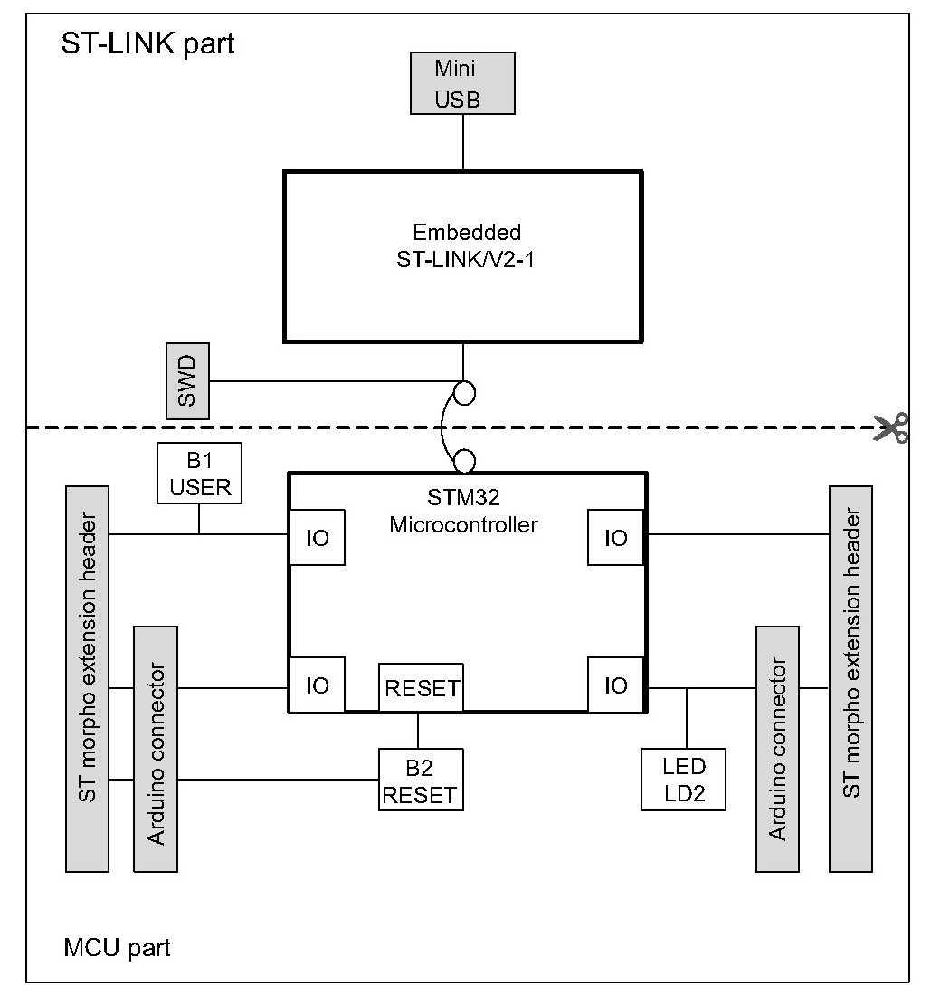
STM32 Nucleo Block Diagram
STM32 Nucleo Board Features
| Features & Specifications | |
|---|---|
| Microcontroller | (32-bit) STM32F401RET6 with ARM Cortex |
| CPU Frequency | 84 MHz |
| VDD (MCU) | 1.7V to 3.6V |
| VIN (BOARD) | 7V to 15V |
| ADC | 12-bit 16Channel |
| Timers | Total 8 Timers (6 of 16-bit, 2 of 32-bit) |
| Watchdog Timers | Available (2) |
| USART | Available |
| I2C | 3 Channels |
| SPI | 3 Channels |
| USB 2.0 | Available |
| Internal Oscillator | Yes, 16MHz |
| External Oscillator Range | 4MHz to 26 MHz |
| On-Board Debuggers | Available |
| Flash Memory | 512Kb |
| SRAM | 96Kb |
STM32 Nucleo Applications
- The board is widely used in the IoT system.
- Nucleo F401RE is friendly to the industrial structure systems.
- In lower power electronics and robots, the board is quick to implement due to its wide research on the internet
STM32 Nucleo F401RE Peripherals
Debug
The board STM32F401RE supports multiple debug methods, which allows the user to test and program the controller in multiple ways. Sometimes method developers can find it difficult due to their limited data on the internet.
USB
The USB can be attached to the board through pins and its USB port. It supports the PC to install the drivers automatically and link the board to it without relying on any third interface. This is not only limited to the STM pin, but it also has an internal burner for both Arduino and STM pins which can be used directly from computers.
Board Cut
The board can be cut into two pieces to minimize its size. The board has two parts one is an STLink and the other is the microcontroller. It could cut down to two pieces and the remaining controller part can be used. After cut it down some power input pins will be specific to some pins and the remaining GPIO will be the same
Indicators
LEDs are used for the indication of the multiple values and data. Some LEDs are directly attached to the GPIO pins to test the simple functions to avoid any extra wires.
2D Diagram
Other Development Boards: