The CD4042 quad “D” latch IC consists of P- and N-channel enhancement mode transistors. It consists of four latches having a common clock input, four buffered inputs and outputs pins. The CMOS logic-based IC’s have the advantage of low power consumption and a wide voltage supply range.
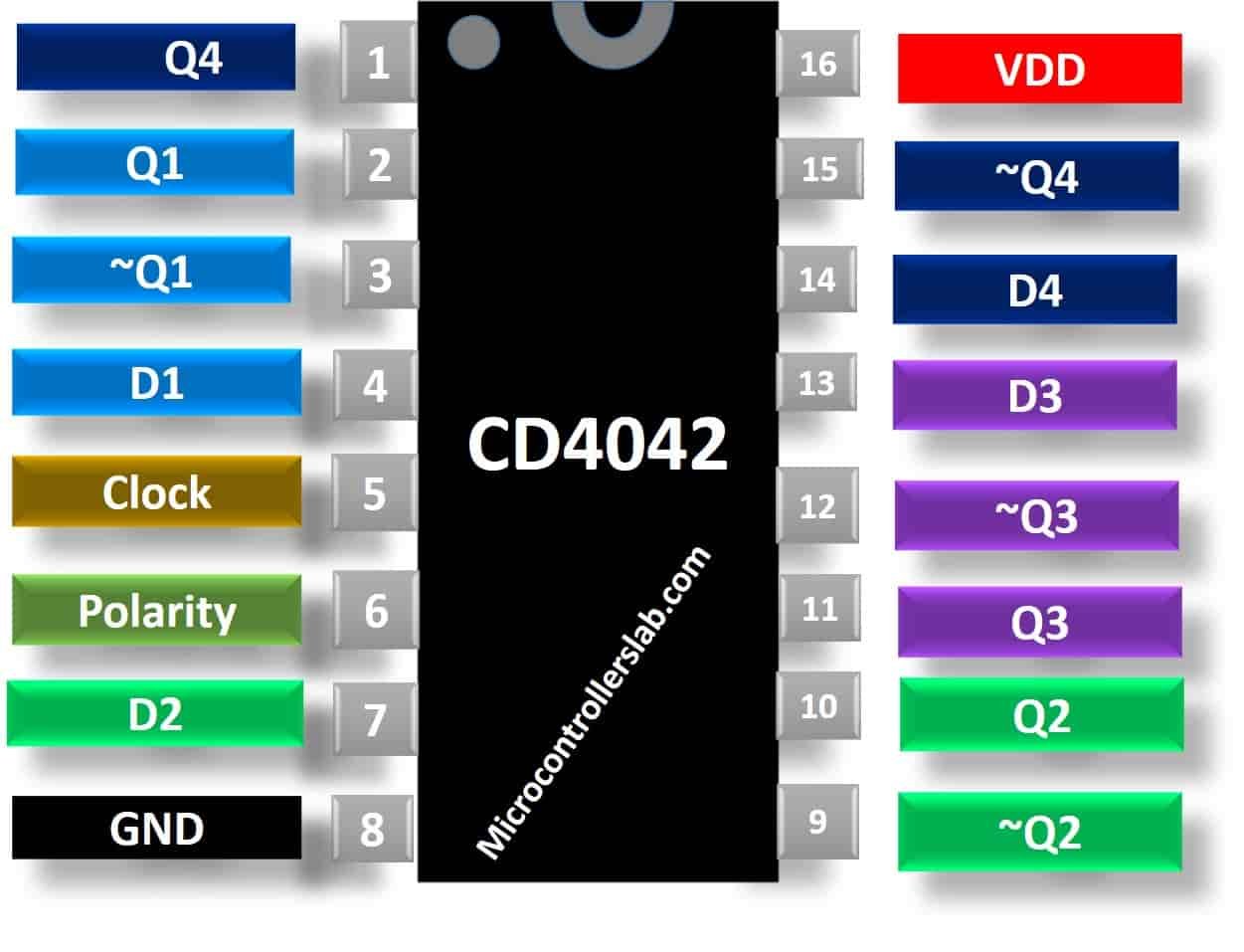
CD4042 Pinout Diagram
As you can see in the pinout diagram that CD4042 has four D latches inside a single chip. Each D latch has one input and two output pins such as Dx, Qx, ~Qx. Here x shows the number of the latch. However, all D latches have common polarity and clock signals. We will see the working of all pins in later sections. The picture shows a pinout diagram.
Pin Configuration Details
CD4042 has a total of fourteen pins. All the pins, their names, and description are mentioned in the table below:
| Pin Number | Pin Name | Description |
|---|---|---|
| 4, 7, 13, 14 | D1, D2, D3, D4 | Four Data inputs |
| 1, 2, 10, 11 | Q1, Q2, Q3, Q4 | Parallel outputs of four latches |
| 3, 9, 12, 15 | ~Q1, ~Q2, ~Q3, ~Q4 | Inverted parallel outputs of four latches |
| 5 | CLOCK | Clock pulse signal provided through a 555 timer IC or any other digital logic IC |
| 6 | POLARITY | We use it to control the rise and fall time of the output. When POLARITY is LOW, the data is transferred to the output at 0 CLOCK level and vice versa. |
| 8 | Vss | Ground of the circuit |
| 16 | Vdd | Positive power supply |
CD4042 Features
- It consists of four flip flops with a common clock Input, normal and inverting Output.
- Low power TTL Compatible
- Clock and Polarity input both controls the output
- Quiescent current specified up to 20v
- Voltage Supply Range: 3V to 20V
- Operating Temperature Range: -55 °C to 125 °C
- Setup Time: 25 to 50ns (vary according to voltage)
- Standard symmetrical output
Equivalent ICS
- 4508: Dual 4-bit Latch
- 4099: 8-bit Addressable Latch
- CD4027 Dual JK Flip Flops IC
- 74LS279
- 74LS373
Where to Use CD4042 Quadruple D Latch?
Latches and Flip flops are basically storage elements. CD4042 IC contains four latches therefore this IC can be used as a storage device for holding registers or in power-switching circuits. It can also be used as input or output ports in Asynchronous systems. This IC can be used for a variety of purposes in electronics.
How to Use CD4042?
Each Latch inside CD4042 consists of 1 data input pin and two outputs Q and ~Q. The change in both outputs value depends on the clock level. In addition to these inputs, it also has a polarity input which is used to program the clock input. When polarity input is LOW, the information present at the data input is transferred to Q and during 0 clock level, and when it is HIGH, the transfer occurs during the 1 clock level.
Internal Block Diagram
The functional diagram of IC CD4042 indicating the parallel data inputs, inverting and non-inverting outputs is shown below.
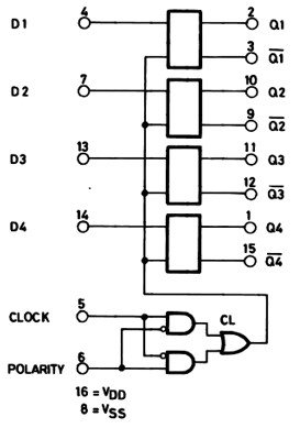
On every clock transition depending on the polarity input, the data is transferred to the outputs but during the same clock level, the value is retained until the value of clock signal changes and becomes opposite to the previous one.
Truth Table
This behavior can be explained through the truth table given below:
| CLOCK | POLARITY | NON-INVERTED OUTPUT |
|---|---|---|
| L | 0 | D |
| Positive edge | 0 | Latch |
| H | 1 | D |
| Negative Edge | 1 | Latch |
You can see from the above truth table that when polarity pin is at LOW state then the output will rise on the positive transition of a clock signal. On the other hand, when it is in a HIGH state.
Polarity Pin Function
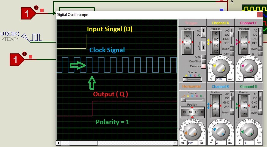
As you can see from the above table, the CD4042 polarity pin decides the transition of D Latch outputs. It decides either output transition will occur on a positive edge of the clock cycle or negative edge. If Polarity signal = 0 or logic Low, it works on a positive edge of the clock and otherwise on the negative edge of the clock cycle.
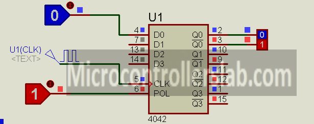
CD4042 Example one
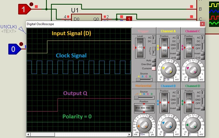
As you can see from this graph when the polarity is equal to active low, an input signal goes high on a positive edge of the clock and output appears on the Q pin on next positive edge of clock cycle.
Example two
Similarly, If the polarity is active high or 1, the input signal appears on the output on the negative edge of the clock. As you can see from the simulation, even though the input signal (D) is available on the positive edge, but it reflects on the output pin on the next negative edge of the clock.
CD4042 Applications
This IC is mainly used in data storage applications. Some of its applications include:
- Digital electronics for data storage
- Bounce elimination switch
- Computers use this IC for computing
- Buffer storage, data transfer, and holding registers
- Used as pulse latches for pulsing the clock quickly
- General Digital Logic
- Used in high circuit designs due to their fast speed
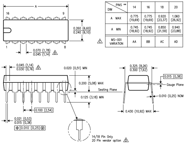
2D Diagram
DataSheet
Related Electronic Components
- PIC18F4550
- CD4022 Divided by 8 Counter
- OP07 Ultra-low offset Voltage Op-Amp
- 74HC157 Quad 2×1 Multiplexer
- CD4017 Counter
- CD4511 BCD to Seven Segment driver
- DAC0808 8-bit Digital to Analog Converter
- MCP3008 8-Channel 10-Bit A/D Converters with SPI Serial Interface
- TL081/ TL082/TL084 JFET-Input Operational Amplifiers