Recommended Components
The following parts are used in this article, along with a generic electronics kit that is handy for building and testing the circuit.
| Component | How it’s used | Buy on Amazon |
|---|---|---|
| ATmega32 microcontroller | The ATmega32 8-bit AVR microcontroller this article covers. | Check Price |
| Electronic component assortment kit (1390 pcs) | A handy assortment of resistors, capacitors, LEDs, diodes and transistors for building circuits. | Check Price |
| Digital multimeter (AstroAI) | Measures voltage, current, resistance and checks continuity while you build and debug. | Check Price |
| Breadboard | Solderless base for prototyping the circuit. | Check Price |
| Jumper Wires | Make the connections on the breadboard. | Check Price |
As an Amazon Associate we earn from qualifying purchases. Prices and availability are accurate as of the date/time indicated and are subject to change.
Pinout Diagram ATMega32
ATMega32 has maximum pins a single microcontroller could have, and all these pins are specified to specific protocols and functions which can be used through programming. All protocols and functions of ATMega32 on different pins are discussed below: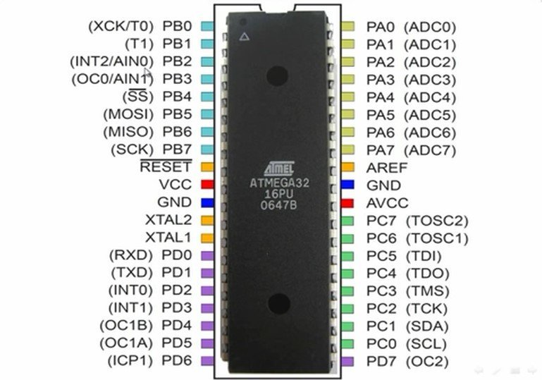 This diagram is an ATMega32 Pin layout of TQFP and MLF Package.
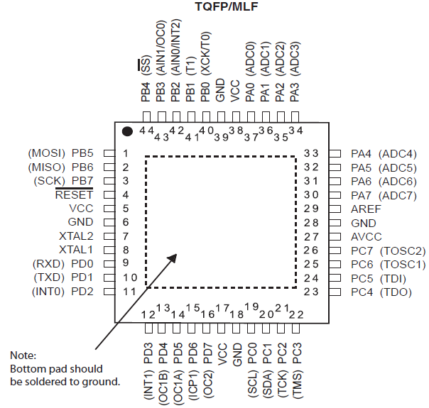
Pin Configuration Details
Digital Input/Output
Input and output pins are the basic need of every device to operate and in ATMega32 there are 32 input/output pins. CMOS device can be used with any I/O pin. The voltage on these pins will not exceed more than the voltage of the applied power and input voltage should not exceed more the power too. All the I/O pins directly come from the Port A, B, C, and D, they also have an internal pull resistor. All I/O pins in ATMega32 are given below:- PA0 – GPIO40
- PA1 – GPIO39
- PA2 – GPIO38
- PA3 – GPIO37
- PA4 – GPIO36
- PA5 – GPIO35
- PA6 – GPIO34
- PA7 – GPIO33
- PB0 – GPIO0
- PB1 – GPIO1
- PB2 – GPIO2
- PB3 – GPIO3
- PB4 – GPIO4
- PB5 – GPIO5
- PB6 – GPIO6
- PB7 – GPIO7
- PC0 – GPIO22
- PC1 – GPIO23
- PC2 – GPIO24
- PC3 – GPIO25
- PC4 – GPIO26
- PC5 – GPIO27
- PC6 – GPIO28
- PC7 – GPIO29
- PD0 – GPIO14
- PD1 – GPIO15
- PD2 – GPIO16
- PD3 – GPIO17
- PD4 – GPIO18
- PD5 – GPIO19
- PD6 – GPIO20
- PD7 – GPIO21
Interrupt Pins
Interrupt pins are the requirements of most of the circuits and it is increasing in number due to the rules of physics. The basic purpose of the interrupt pins is to get the attention of the CPU when every external device required. The controller requires an external pulse on specific pins and then the CPU will perform the programmed instructions by putting all other instructions at hold. In ATMega32 the number of interrupt pins is three. All these pins are useable without affecting each other. All interrupt pins within ATMega32 are:- INT0 – GPIO16
- INT1 – GPIO17
- INT2 – GPIO3
ATMega32 Serial Communication Ports:
Asynchronous Serial
ATMega32 supports multiple kinds of serial communication protocol and asynchronous serial communication is one of them. UART Communication is quite popular in most of the peripherals due to its simplicity and dependent on the programming. It communicates with two-pin, one for sending data and second for receiving it. In this microcontroller, there is a module for asynchronous serial communication which is given below:- RXD – GPIO14
- TXD – GPIO15
Synchronous Serial
Asynchronous and Synchronous serial communication systems are mostly the same but in asynchronous the devices use the internal program for clock and in the synchronous and external clock input/output pins are required to keep the data sync between two devices. In ATMega32 there is a pin for external clock input/output during serial communication.- XCK – GPIO1
SPI
SPI protocol is also a popular serial communication due to its managing ability of different devices at a single time. It uses four wires, two for data and one for clock but the forth wire can be used in case of multiple devices. Whenever multiple devices need to operate with ATMega32 then only forth pin (SS) will be increased and the number of data and clock pin will be the same. ATMega support only four pins for single SPI communication device but in case of multiple devices Select Slave pin can be made through programming.- SS’ – GPIO5
- MOSI – GPIO6
- MISO – GPIO7
- SCK – GPIO8
I2C
It is also a kind of serial communication but it is mostly used in those devices which requires only one-way communication most of the time. It is quite popular in most of the sensors, LCD, and motors too. I2C pins use one wire for data and second for the clock pulse, both these pins are given below:- SCL – GPIO22
- SDA – GPIO23
Analog to Digital Channel
There is a total of 8 analogs to digital channels that can be used as ADC. These all channels use a single 10-bit ADC which can be used by multiple channels at the same time. The channels are only in port A and all are listed below:- ADC0 – GPIO40
- ADC1 – GPIO39
- ADC2 – GPIO38
- ADC3 – GPIO37
- ADC4 – GPIO36
- ADC5 – GPIO35
- ADC6 – GPIO34
- ADC7 – GPIO33
Timer Module Pins
In ATMega32 there is a total of three timers. The first two timers are 8-bits and the third timer is 16-bit. Timer0 and Timer1 can only operate with the external pulse, timer1 only operate within the microcontroller. All these timers can use internal and external oscillator, but they also can use the sperate oscillator. The sperate oscillator will be given through the specific pins. All these oscillator and timer pins are given below:- T0 – GPIO1
- T1 – GPIO2
- TOSC1 – GPIO28
- TOSC2 – GPIO29
Capture/Compare/PWM
Some pins within the microcontroller can be used to generate the desired output signal. These pins capture the input signal and then compared it with the instructed signal and then it generates an event on the match. These pins are mostly used for PWM generation. All these pins in ATMega32 are:- OC0 – GPIO4
- OC1B – GPIO18
- OC1A – GPIO19
- OC2 – GPIO21
ICP
PWM pins only for output, but there is an input pin for PWM know as ICP. This can be used to capture the external input and then it can be used further to calculate the frequency and duty cycle of the external device.- ICP1 – GPIO20
Comparator Pins
ATMega32 has an internal comparator that can be used to compare an analog input signals. It has two pins, one is used for a non-inverted signal and the second is used for the inverted signal. Internal registers can use the analog compared signal. All these pins are given below:- AN0 (non-inverted) – GPIO3
- AN1 (inverted) – GPIO4
JTAG Programmer Pins
JTAG pins were introduced by the company to debug or to test the microcontrollers. ATMega32 has JTAG communication pins, that can also be used to program the microcontroller. All JTAG pins are given below:- TDI – GPIO27
- TDO – GPIO26
- TMS – GPIO25
- TCK – GPIO24
Power Pins of ATMega32
AREF
The ADC of ATMega32 uses the power supply of microcontrollers to measure the different levels of the analog input signals. This function sometimes starts giving unexpected values. The maximum value of the analog signal will be given on the.reference pin as voltages.- AREF – Pin32
AVCC
Analog to Digital converter of the microcontroller required an external voltage input to activate so it can operate. ATMega32 analog power pin is:- AVCC – GPIO30
Power Input
Every device requires power to operate. ATMega32 has three power pin. One is for power input and the others for ground. All power pins are:- VCC – GPIO10
- GND – GPIO11, GPIO31
Oscillator
ATMega32 has an internal 8MHz clock that is extendable by using external clock pins. External clock pins can extend the clock up to 16MHz.- XTAL2 – GPIO12
- XTAL1 – GPIO13
Reset
ATMega has an external reset pin to reset the device by external devices and buttons. The reset pin in ATMega32 is:- RESET’ – GPIO9
Alternative Microcontrollers
Atmega16, Attiny45, Attiny85, Attiny88ATMega32 Block Diagram
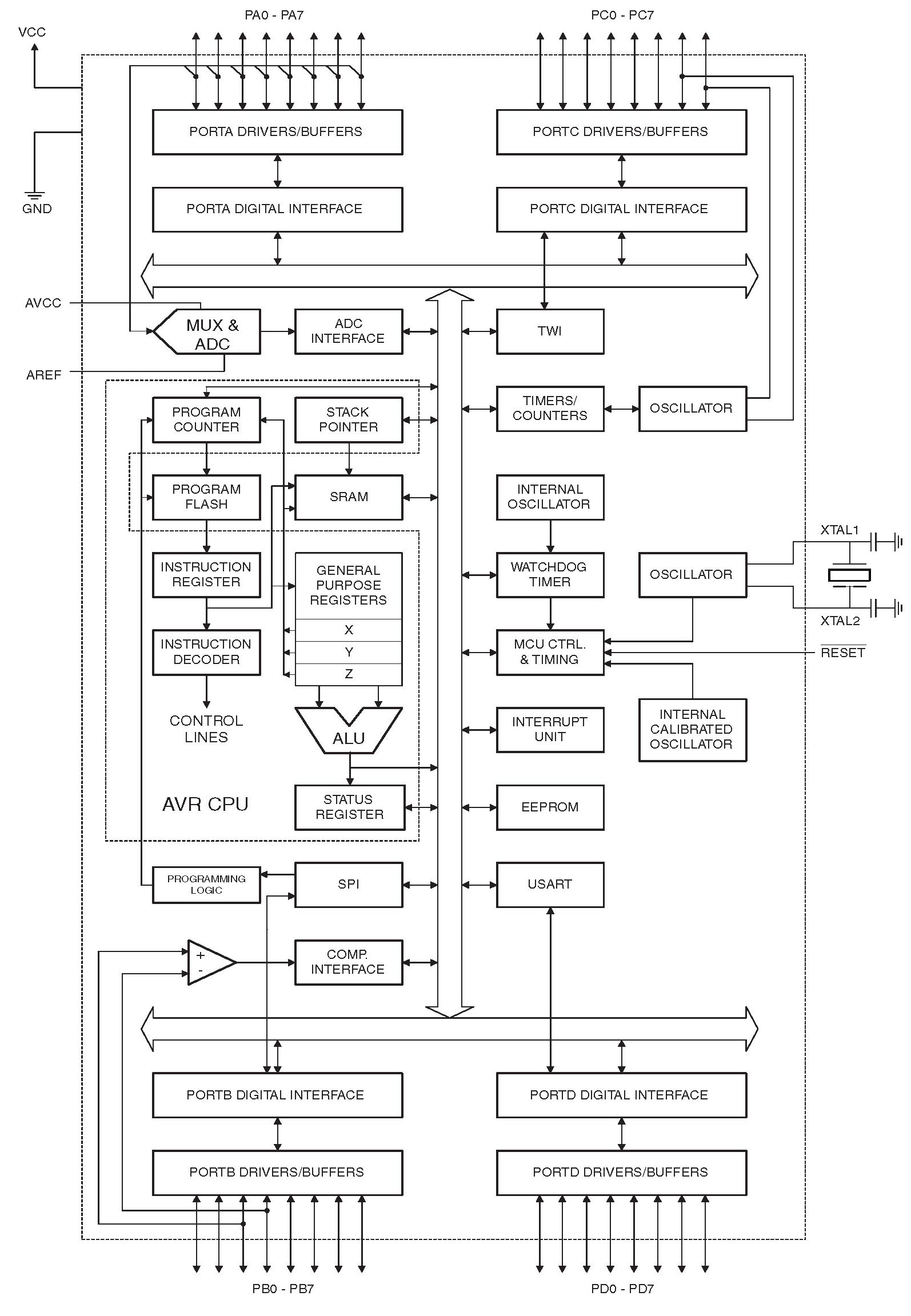
Block diagram provides an overview of all peripherals such as GPIO Ports, Communication ports and interrupts pins. This also shows an interface of the data bus and address bus with these internal peripherals. ATmega32 Main Features and Specifications
| FEATURES & SPECIFICATIONS | |
|---|---|
| CPU Architecture | 8-bit RISC Architecture |
| CPU Frequency | 16MIPS |
| Operating Voltage Range | (4.5V – 5.5V) |
| GPIO PORTS | 32 I/O Pins |
| Interrupts | 3 |
| Timers | 3 (Two 8-bit and one 16-bit timer) |
| PWM | 4 |
| ICP | One ICP Pin |
| Synchronous Serial | One Channel |
| Asynchronous Serial | One Channel |
| I2C | One I2C channel |
| SPI | One SPI channel |
| JTAG | Available |
| Boot loader | Available |
| Watchdog timer | Available |
| LAN | Not Available |
| CAN | Not Available |
| ADC | 8 Channel, 10-bits |
| SRAM | 32Kb |
| FLASH (Program Memory) | 1024Kb |
| EEPROM | 512 bytes |
| Comparator | 1 |
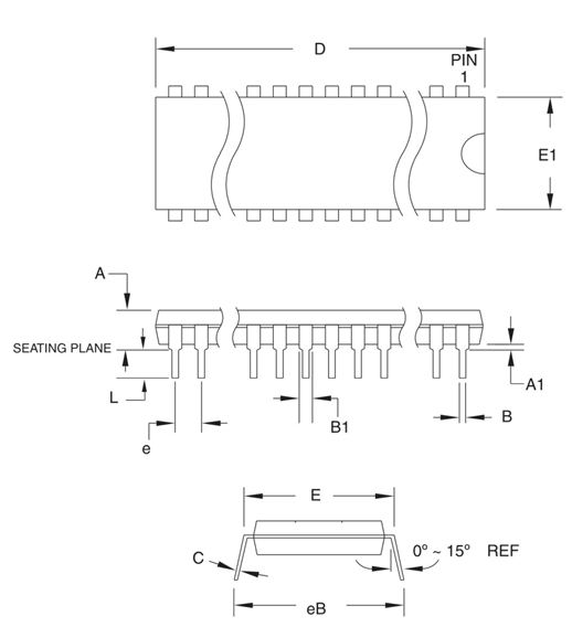
| Packages | PDIP (40-Pins), TQFP (44-Pins) & MLF (44-Pins) |
Atmega32 Programming
Before you start with the programming of this microcontroller, you must have a clear understanding of GPIO pins. Therefore, we list all pins description earlier. Following these steps to start with embedded programming.- Firstly, Download an integrated development environment (IDE) that has a built-in compiler for your selected microcontroller
- Select a Programmer that we will use to upload code to Atmega32
- Write your first simple program such as LED Blinking and upload code.
- After building code, building a circuit of LED interfacing and provide power
- You will see an LED blinking according to the rate you have defined in program
Programming Examples
Follow these tutorials starting from downloading a compiler to writing your program for your first project:- ATMEL STUDIO 6 TUTORIAL step by step guide
- LED BLINKING using ATMEGA32 AVR microcontroller
- How to use push button with ATMEGA32 AVR microcontroller
- LCD interfacing with ATMEGA32 AVR MICROCONTROLLER
- DC motor interfacing with atmega32 and L293
Atmega32 Project
Applications
- ATMega32 is suitable for digital signal processing.
- Most of the Peripherals uses the ATMega32 as an interface in industrial systems.
- To make the interface between two kinds of peripherals microcontroller ATMega32 is the best choice.
2-D Diagram
I WOULD LIKE TO KNOW MORE ABOUT ATMEGA32 PROGRAMMING IN ASSEMBLER. I AM FACING PROBLEM IN PROGRAMMING TIMER/COUNTERS.