In the last tutorial, we saw how to design a half adder circuit in LabVIEW. In this tutorial, you will learn how to design a full adder circuit in LabVIEW. If you are familiar with digital logic design, you should know the purpose and working of a full adder in digital logic design or digital systems. It is similar to the half-adder we discussed in the previous tutorial. I will help you design a VI that will take two binary inputs from the user and return the sum and carry after adding them. At the beginning, a brief introduction to the full adder is provided. After that, a VI is designed to perform the full adder operation for three binary inputs. At the end of the tutorial, you are provided with an exercise to do on your own.
Design Full Adder Circuit in LabVIEW
In order to add three binary digits, we will need an adder, namely a full adder circuit. This adder will take three binary digits as input and, at the output, it will return two outputs named sum and carry. The implementation of a full adder is a little more difficult than a half adder, as you will see shortly in the programming portion. A full adder has three inputs and two outputs, whereas a half adder has two inputs and two outputs. This is the main difference between a half adder and a full adder.
Full Adder Circuit in LabVIEW Example
First of all, create a VI as we have discussed in tutorial 1 and save it for future use, as we have been doing in all the previous tutorials. Now we need to set three Boolean inputs for the values A, B, and C that will be added, and two Boolean outputs to display the sum and carry. For the Boolean inputs, we will use a Boolean control, specifically a push button. On the front panel, right-click and select Boolean from the control palette, then choose Push button, as shown in the figure below:

Figure 1: Boolean controls placement
Place three push buttons for two binary single-digit inputs. Now, in order to place an indicator for the binary output indication, we have to add LEDs. On the front panel, right-click and from the control palette, select Boolean. Then, choose Round LED as shown in the figure below.
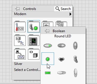
Figure 2: Boolean indicator
Place two indicators, also display the sum, and carry on the output. The resulting controls and indicators are shown in the figure below.
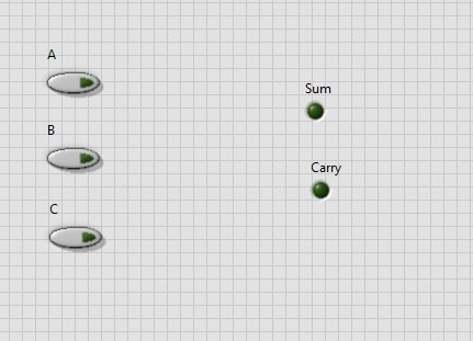
Figure 3: Control and indicators
Now move to the block diagram for XOR, OR, and AND gate placement. From the function palette on the block diagram window select Boolean and then select Exclusive Or as shown in the figure below,
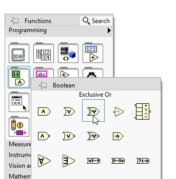
Figure 4: Exclusive Or placement
Place two such blocks as we are interested to do the XOR operation on three inputs. The output of these blocks will return the sum of the full adder output.
At the input of the first block, connect the two Boolean controls A and B. Connect its output to the input of the next XOR block. Then, connect the C control to the remaining input node of the second XOR gate. At the output of the second XOR gate, connect the Boolean indicator (the round LED) that you have previously created and named as “sum.” The figure below shows the correct connections:

Figure 5: Summing block of full adder
To do the carry operation we have to use two AND and one OR gates. From the function palette on the block diagram window select Boolean and then select AND as shown in the figure below,

Figure 6: And block placement
At the input of this AND gate, connect the output of the first XOR gate and the C control. Place another AND gate with inputs connected to A and B control. Now, from the function palette on the block diagram window, select Boolean and then select OR as shown in the figure below:

Figure 7: Or block placement
At the inputs of these or blocks connect the output from the two and gates and at the output node of this block connect the indication of output carry as shown in the figure below,

Figure 8: Carry block of full adder
The complete block diagram of a full adder is shown in the figure below,

Figure 9: Block diagram
The output of the full adder should be according to the table given below:
| A | B | C | Sum | Carry |
| 0 | 0 | 0 | 0 | 0 |
| 0 | 0 | 1 | 1 | 0 |
| 0 | 1 | 0 | 1 | 0 |
| 0 | 1 | 1 | 0 | 1 |
| 1 | 0 | 0 | 1 | 0 |
| 1 | 0 | 1 | 0 | 1 |
| 1 | 1 | 0 | 0 | 1 |
| 1 | 1 | 1 | 1 | 1 |
Now on the front panel, set the values of both A, B, and C as 0 and run the VI, both the LEDs will remain of as according to the above table, as shown in the figure below,

Figure 10: Output 1
Now change the values and test the VI for different combinations of inputs as shown in the figure below,

Figure 11: Output 2
Exercise
- Test the designed circuit for all the remaining combinations from the table and verify the output from the table.
Conclusion
In conclusion, we have learned how to design a full adder circuit in LabVIEW. A full adder is a crucial component in digital logic design and digital systems, as it allows us to add three binary digits together, producing a sum and a carry output. Through the step-by-step process outlined in this tutorial, we have constructed a VI that takes user inputs and provides the corresponding sum and carry values. By understanding the differences between a half adder and a full adder, and implementing XOR, OR, and AND gates in LabVIEW, we have successfully designed a functional full adder circuit. This tutorial serves as a foundation for further exploration into the realm of digital logic design and its practical applications.