TL494 is a PWM controller IC used for power electronics circuits. It comprises of on-chip two error amplifiers an oscillator with adjustable frequency feature, an output flip-flop having pulse steering control, and an output control circuit with feedback. The error amplifiers can compensate voltage from –0.3 to VCC – 2 volts in common voltage configuration. The comparator controls the dead-time with a fixed offset. The dead-time comparator offers almost a 5% range. The external oscillator can also provide a reference frequency signal to this PWM IC. Users can bypass an on-chip oscillator by connecting RT to the reference output pin.
In this tutorial on TL494, you will learn these concepts?
How to use the TL494 pulse width modulation control IC? How we can use TL494 pulse width modulation control IC to generate fixed and variable PWM. I have already posted a tutorial on sg3525 pulse width modulation controller. You may also like to check it. TL494 is a PWM control or generation integrated circuit. TL494 is used in many applications. I have designed a proteus simulation on how to generate PWM signals and how to design a buck converter. It can be used in dc to dc converter circuits. It is also used in pure sine wave inverter circuits. I have made many power electronics-based projects. You may also like to check them:
- Pure sine wave inverter using pic microcontroller
- single phase pure sine wave inverter using Arduino
- Three-phase sine wave inverter using Arduino
- dspic microcontroller based pure sine wave inverter
- Modified sine wave inverter using pic microcontroller
- Solar inverter using sg3525
Introduction to TL494 PWM control IC
It is a complete PWM control IC. It can be used in single-end operation as well as in push-pull configuration. It also provides variable dead time which provides a maximum range of PWM. It has all the functions required to design a power supply circuit. Block diagram of TL494 is shown below:

It is a fixed frequency and a variable PWM IC. Pulse width is varied by comparing the sawtooth waveforms of two internal oscillators on the timing capacitor to any one of the control signals. The output becomes high when the control signal becomes lower than the voltage of the sawtooth waveform. I recommend you to check the datasheet of TL494 PWM control IC for more information and working details.
Pinout of TL494
The Pinout diagram and pins details of TL494 is given below. We provide a Pinlayout description and working in later sections.
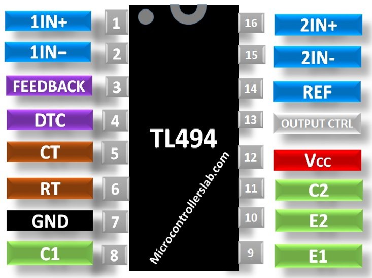
This table lists the pin configuration of the pulse width modulation control circuit.
| Pin number | Pin name | Pin Configuration |
|---|---|---|
| 1 | 1IN+ | Input 1 for error amplifier one ( Non-Inverting) |
| 2 | 1IN- | Input 2 for error amplifier one ( Inverting) |
| 3 | FEEDBACK | Feedback connection pin from outputs |
| 4 | DTC | Input for dead-time control comparator |
| 5 | CT | Capacitor terminal to set frequency |
| 6 | RT | Resistor terminal to set frequency |
| 7 | GND | Ground pin for power supply |
| 8 | C1 | Collector pin of Output 1 |
| 9 | E1 | Emitter pin of Output 1 |
| 10 | E2 | Emitter pin of Output 2 |
| 11 | C2 | Collector pin of Output 2 |
| 12 | VCC | Positive Power supply pin |
| 13 | OUTPUT CTR | Select output mode from three options |
| 14 | REF | Reference for 5 volts regulator |
| 15 | 2IN- | Input 1 for error amplifier two ( Inverting) |
| 16 | 2IN+ | Input 1 for error amplifier two ( Non-Inverting) |
TL494 Features
- Built-in PWM control Channels
- Current sink and source rating: 200mA
- Dual output selectable operations: Single-ended or push-pull operation
- Deadtime control feature: Variable range
- Easy synchronization with other circuits
- PWM outputs: 2
- Fixed frequency oscillator
Electrical Specifications
- Supply voltage ( Vcc): up to 41 volts
- Maximum output current for both PWMs: 250mA
- Output voltage at collector pins: 41 volts
- Temperature range: -65 to 150 degrees
For further information on timing diagrams and electrical specification, download datasheet
How does the PWM controller work?
As mentioned earlier, it is a fixed frequency and variable duty cycle dual PWM control circuit. It does not require any external components to operate except a few resistors and capacitors for an oscillator. This oscillator is responsible for generating a sawtooth waveform according to timing capacitor CT. This TL494 IC generates signals by comparing a sawtooth waveform with two control signals of the error amplifiers. The output signal will be on during the time when sawtooth voltage is greater than the voltage at error amplifiers outputs. You can see a block diagram given above.
- Output signal low: if sawtooth voltage less than the control signal voltage
- Output signal High: if sawtooth voltage greater than the control signal voltage
Pulse-Steering Flip-Flop transfers the PWM output signal to output transistors.
How to select oscillator Frequency?
In the last section, we see that the oscillator is mainly responsible for generating sawtooth waveform. This sawtooth waveform used for deadtime control and PWM comparator amplifiers. Therefore, the frequency of the oscillator determines the frequency of output signals. Now, we will see how to choose the frequency of an oscillator.
We can select frequency by selecting suitable values of RT resistor and CT capacitor. We can select the capacitor and resistor values according to this formula:
Frequency= 1/ RT X CT
TL494 Examples
First, we will see a simple example to generate pulse width modulation signals from this IC. After that, a practical example provides a circuit diagram of a buck converter.
Circuit diagram to generate PWM signals
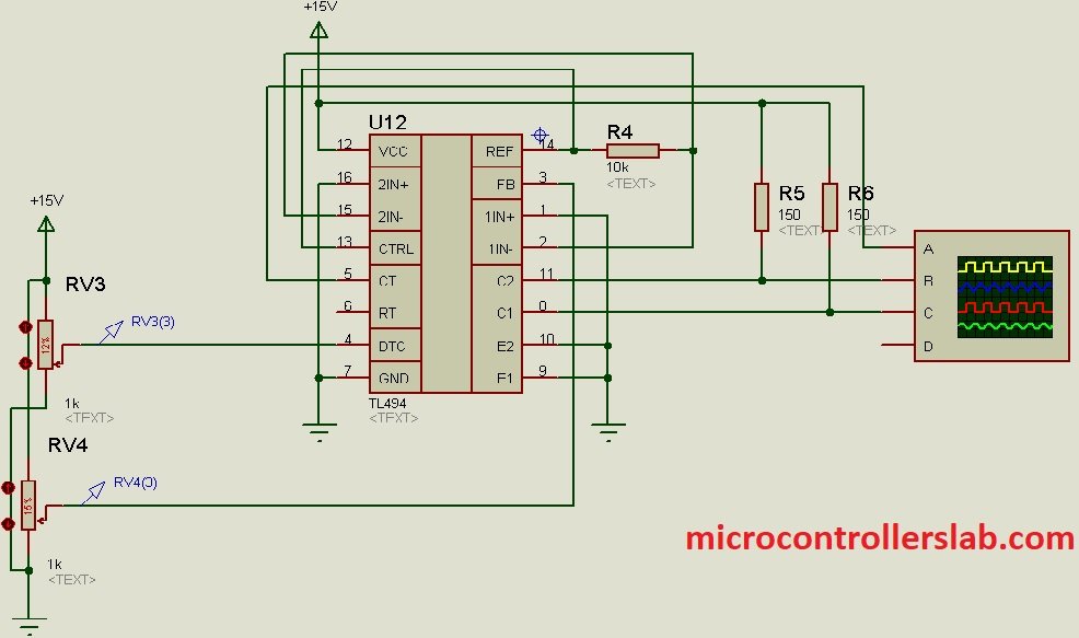
Below circuit diagram can be used to generate 2 PWM signals. The width of each PWM can be controlled through these variable resistors.
Simulation results of two PWM are shown below:

Buck converter design Example

We have designed a buck converter using TL494 as an example. Input to buck converter is 25 volt and output is in the range of 7 to 19 volts. Users can change the output voltage with the help of the variable resistor shown in the circuit diagram below. TIP127 is used as a switching device.
For detailed working of buck converter check the video simulation. In this video, I have explained the working of buck converter design using this pulse width modulation controller circuit. I have used a variable resistor to control the duty cycle of the pulse width. Another variable resistor is used to control the current. Input voltage is 25 volt and the output voltage is in the range of 5 volts to 19 volts. When the duty cycle is maximum output voltage will be 19 volts and when the duty cycle is minimum, the output voltage will be 5 volts. The voltage divider circuit is used for feedback voltage measurement and a shunt resistor is used for feedback current measurement.
TL494 Applications
- Switch Mode Power Supplies
- High Power Inverters
- Power Electronics Applications
- Power factor correction meters
- Desktop and Portable applications
Packages
This IC is available in four different 16 pin packages such as SOIC, PDIP, SOP, TSSOP. You can check the datasheet for the 2D physical dimension diagram of these packages.
Thanks Bilal .
Sir I want to three phas inverter please contact
Hi sir,pls where can I get your inverter circuitdiagram to buy.Thank you
Hi sir,please where can I get your circuit to buy.Thank
Noble friend,
I need you to teach me how to make a BOOST CONVERTER that takes a 12v voltage from a standard lead acid battery, and turns that voltage to 20V on your output, would you know how to teach me how to do this on the PROTEUS SIMULATION SOFTWARE?
I really need to learn how to do this please look forward to your hello …
ENDEL
i like this diagrams, but my tl494 inverter output ll
always increase up to 385v as the sun rises or increases. plz help me. thanks
BOA NOITE GOTEI DA ESPLICASAO GOSTARIA DE SABER O SG3524N E = O UC3843