Sine wave inverter circuit diagram with a complete step-by-step program and coding. In this article, we will discuss how to use a push-pull converter, sinusoidal pulse width modulation, an H-bridge, and a low-pass LC filter to create a pure sine wave inverter circuit diagram. I have already discussed all of these topics in the following articles.
We suggest you go through the following articles before reading this one.
- Pure sine wave inverter: A-Z guide to making an inverter
- How to use MOSFET DRIVER 1R2110
- DC-DC converter using push-pull topology
- How to make an H bridge and diagnose problems
- SPWM generation using PIC16F877A microcontroller
Pure Sine Wave Inverter Introduction
A pure sine wave inverter is a device that converts DC (direct current) power from a battery or other power source into AC (alternating current) power with a smooth and pure sine wave output. This type of inverter is commonly used in applications where sensitive electronics or appliances require a high-quality power supply that mimics the utility grid.
Unlike modified sine wave or square wave inverters, a pure sine wave inverter produces a waveform that closely resembles the smooth sinusoidal waveform of the AC power provided by utility companies. This makes it compatible with a wide range of devices, including sensitive electronics such as laptops, smartphones, and medical equipment. It also ensures that the connected devices operate efficiently and without any humming or interference.
Pure sine wave inverters are commonly used in off-grid or backup power systems, RVs, boats, and solar power systems. They provide reliable and clean power, which is essential for running sensitive equipment and appliances smoothly.
Pure Sine Wave Inverter Circuit Diagram and Working
In our last article on SPWM generation, we discussed how to implement sinusoidal pulse width modulation using a microcontroller and how to select the number of pulses and duty cycle for each pulse. We used the PIC16F877A microcontroller to write the code for SPWM. You can use any microcontroller of your choice, but the procedure will remain the same as we discussed in the last article on SPWM generation.
We have used 100 pulses, and the frequency of each pulse is 20 kHz. Hence, the timer period of each pulse is equal to 2 * 50 µs = 100 µs. Therefore, we have used 100 pulses as we mentioned in the previous article. The greater the number of pulses, the more pure sine wave will be produced. We have calculated the duty cycle for 100 pulses using the same method we discussed earlier. Array of the duty cycle is:
duty cycle for hundred pulses = {0, 8, 16, 24, 31, 39, 47, 55, 62, 70, 77, 85, 92, 99, 106, 113, 120, 127, 134, 141, 147, 153, 159, 165, 171, 177, 182, 188, 193, 198, 202, 207, 211, 215, 219, 223, 226, 229, 232, 235, 238, 240, 242, 244, 246, 247, 248, 249, 250, 250};Code
The code for this project is written in the MIKROC compiler and 8Mhz crystal is used in this project. If you do not know how to use MikroC for Pic, you can refer to these tutorials:
- How to Use “MikroC PRO for PIC” to Program PIC Microcontrollers
- Pic microcontroller programming in c using Mikroc Pro for PIC
const unsigned char SinLkUpTab[50]= {0, 8, 16, 24, 31, 39, 47, 55, 62, 70, 77, 85, 92, 99,
106, 113, 120, 127, 134, 141, 147, 153, 159, 165, 171, 177, 182, 188, 193, 198, 202, 207,
211, 215, 219, 223, 226, 229, 232, 235, 238, 240, 242, 244, 246, 247, 248, 249, 250, 250};
unsigned short cnt,inc,dec,sqinc,cnt1;
void interrupt()
{

if (dec==0)
{cnt++;
PWM1_Set_Duty(SinLkUpTab[cnt]);
}
else if (dec==1)
{cnt–;
PWM1_Set_Duty(SinLkUpTab[cnt]);
}

TMR1IF_bit = 0; // clear TMR0IF
TMR1H = 0xFF; // Initialize Timer1 register
TMR1L = 0x76;
}
void main()
{
TRISB = 0; // designate PORTB pins as output
PORTC = 0; // set PORTC to 0
PORTB = 0; // set PORTC to 0
TRISC = 0; // designate PORTC pins as output
TRISA = 0; // designate PORTB pins as output
PORTA = 0; // set PORTC to 0
T1CON= 0b00000001; // Timer1 settings
TMR1IF_bit = 0; // clear TMR1IF
TMR1H = 0xFF; // Initialize Timer1 register
TMR1L = 0x76;
TMR1IE_bit = 1; // enable Timer1 interrupT
cnt = 0; // initialize cnt
*** Note: This is not a complete code
You can contact us at microcontrollerslabhub@gmail.com to purchase code and simulation.
Pure Sine Wave Inverter Circuit Simulation Results
Demonstration
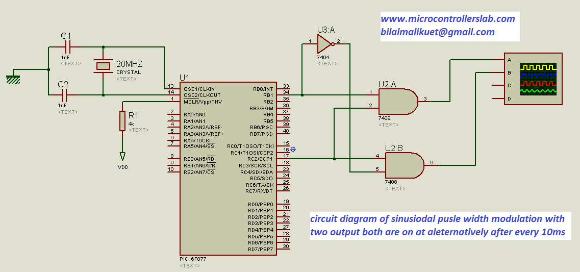
The diagram below shows the circuit diagram of sinusoidal pulse width modulation with two outputs that are on alternatively after every 10 ms.
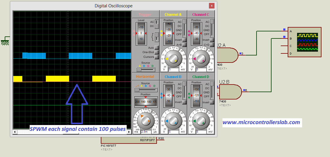
The output of the SPWM circuit diagram
Gating signals for H bridge
Now we will discuss how to use the above circuit for generating four gating signals for an H-bridge, which we have already discussed in the above articles. We have taken two more outputs from the same circuit to generate four gating signals for the H-bridge. The circuit diagram is shown below:
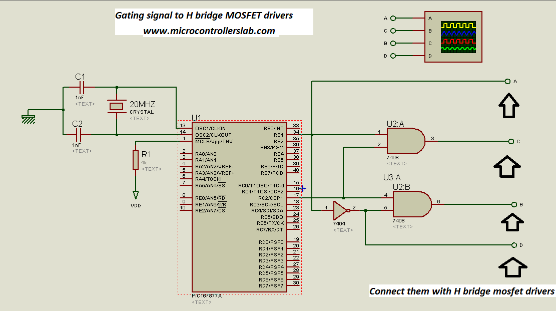
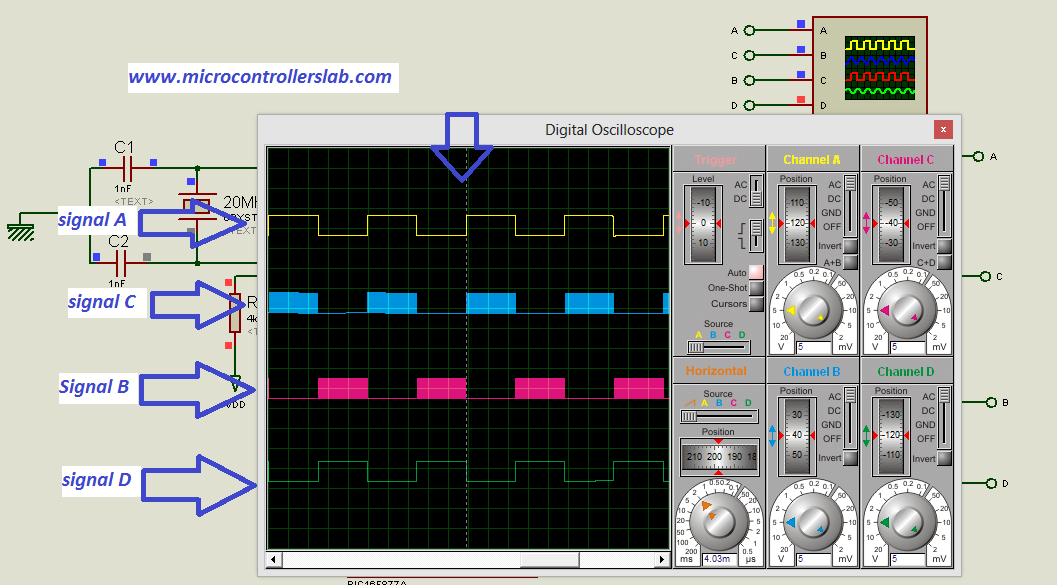
The output of SPWM circuit gating signals for H bridge:
Use the above circuit to drive the MOSFETs of the H-bridge through MOSFET drivers IR2110. I have explained everything about pure sine wave inverters using switch mode techniques. Starting with a basic overview of pure sine inverters and their types. After that, I have discussed the use of the voltage mode PWM controller SG3525 and its applications. Then, I explained the MOSFET driver IR2210 and its usage. I also discussed a DC-to-DC converter using the push-pull topology and how to create an H-bridge using IR2110. I have written a detailed article on sinusoidal pulse width modulation. Now, you can utilize all the knowledge you have gained to create a pure sine wave inverter. Simply connect a low-pass filter at the output of the H-bridge, and you will obtain a clean and precise pure sine wave output.
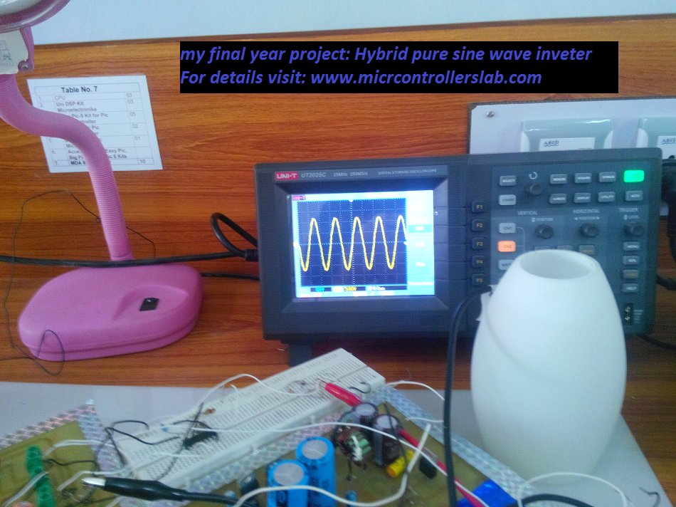
I have obtained a pure sine wave in my final year project, “Hybrid Pure Sine Wave Inverter,” by connecting an LC filter at the output of the H Bridge. The LC values I used are L = 2mH and C = 3.3uF. The diagram illustrating the pure sine waveform I achieved in my final year project is shown in the figure below:
NOTE: It is difficult to simulate this circuit in Proteus. You can easily obtain a pulsating wave output result in Proteus. However, when you connect an LC filter at the output of the H Bridge, Proteus will not simulate your circuit. We suggest you make this circuit on hardware and verify the results.
Conclusion
In conclusion, this article provided a comprehensive overview of how to create a pure sine wave inverter circuit diagram. It covered topics such as the use of a push-pull converter, sinusoidal pulse width modulation, an H-bridge, and a low-pass LC filter. Key concepts and considerations were explained, including the selection of pulses and duty cycle for each pulse. The article also highlighted the importance of using a pure sine wave inverter for powering sensitive electronics and appliances, along with its applications in off-grid or backup power systems, RVs, boats, and solar power systems. Furthermore, the article delved into the intricacies of generating gating signals for the H-bridge and emphasized the use of MOSFET drivers for this purpose. Overall, with the knowledge gained from this article, readers can confidently design and construct their own pure sine wave inverter systems, ensuring a reliable and clean power supply for their specific needs.
You may also like to read:
Hi BILAL ALI AHMAD,
I appreciate your efforts in providing complete explanation. It is really loud and clear I would say. May ALLAH Almighty Bless You and support you in all your endeavors.
Ameen 🙂 Thanks for nice words.It pleasure for me.
Now I am writing series of articles on GSM interfacing with microcontrollers and 2-3 projects related to GSM like home automation system, wireless temperature sensor etc. Keep visiting my blog for more information on GSM.
AOA
Dear brother, Hope you are fine. I’m final year student at UET Taxila. I’m working on a project “VFD” in which I’m using the same method you described above, but I’ve never worked on PIC microcontrollers, I’m familiar with AVR mega32 micro controller only. I need to generate the same waveform of 50Hz SPWM for VFD so I need code for ATmega32 micro controller. I’m using AVR Studio 6 as compiler. Plz contact me if you can help. I need it ASAP. Thanks in advance. Stay blessed.
you can use the same method for every microcontroller
I need program and complete circuit bro for my univ project
Hi BILAL ALI AHMAD,
I was been trying to design a Sine Wave Inverter for a long time. Initially, I had issues with using IR2110. I’m settled with that now. My hardware is already same as yours. I tried using your code. My output is not even closer. Sine wave looks like it gradually increases, then flatted at the top and just few spikes at the negative half cycle. I also designed a filter and I’m satisfied with its filtering. But One will hardly believe it is a sine wave. Could you please help me with this?
There might be issue with your h bridge. First debug your H bridge.Follow these step:
1) check gating signals to IR2110
2) check output from IR2110. level of your gating signals should increase to about 10 volt. voltage level of spwm should be 5 volt from microcontroller.
3) check input singals to gate of mosfet and its voltage level
4) Check output at drain at output of H bridge. there should be two spwm singals and should be on at alternatively after 10ms.
5) now check output after connecting Low pass LC filter
if you are not getting any of above results .then There is a issue with your H bridge. Fix it first..
Hi BILAL ALI AHMAD,
That was incredible support from your side. My output at high side is not perfect, Let me fix that first. Thanks for your help.
It will be pleasure for me if your project work properly..
Good luck
Hi BILAL ALI AHMAD,
I settled gate driver issue. But it doesnt seem to work 🙁
hi emaniac i need this project code ,if you having please send my mail id jaisurya446@gmail.com
because i dont have more money so please help me
am waiting for your reply
thank u
Hi BILAL ALI AHMAD,
Was just referring your code and found this.
why don’t you just
initialize
PORTB.B1 = 0;
PORTB.B2 = 1;
and generate 2 complementary square waves
else if (cnt==0 &&dec==1)
{
PORTB.B1 =~PORTB.B1;
PORTB.B2 =~PORTB.B2;
dec=0;
}
This would eliminate the need of a NOT gate right?
yes you can modify it.
Hi BILAL ALI AHMAD,
I’m really happy that you helped me. My problem was with the driver. And I successfully solved it. I’m now able to get a pure and clean sine wave. Thank you for your support.
welcome 🙂
Its pleasure for me,my articles helped you to achieve your required output.
Hi
Nice blog. Loving it. God bless u.
Scope use at output how?
can u pls explain?
I didn’t understand what you want to ask?
you mean how to use scope to see sine wave at the output of pure sine wave inverter?
simply connect oscilloscope across capacitor of LC filter.
if you asking any other thing , you are welcome to comment again.
what to the ground pins or the alligator clips?
not sure. pls help
connect LC filter at the output of H bridge and connect scope one terminal with common point of LC filter and other any other terminal of LC filter. In other words connect scope across capacitor of scope. DC ground of battery should have no connection with output of LC filter
Thank you, I connect it. It shorts. why?
You must had connected across same terminals. There might be issue with your LC filter connection. You wasn’t made LC filter connections properly.. Post picture of your LC filter connection with H bridge
Hello Sir i see u are giving us a lot of help which we dont get online its like top secrct nobody wants to help on sine wave inverter. I am trying to build a sine wave from analog components sir if i get ur email I can send u the circuit so u can check through for me because I am having some heating in the fets Sir and I would really appreciate ur help thank u
Send me circuit diagram on my email I will check it
microcontrollerslabhub@gmail.com
After building the programe, I received the message below, may you help me?
Line Message No. Message Text
12 402 ;expected, but “-” found
12 424 “}” expected “;” found
14 424 ‘}’ expected ‘}’ found
0 102 Finished (with errors): 10 Jul 2015, 14:04:05 MyProject.mcppi
Thank u very much Sir I willsend to u now
Did uget the circuit sir
I got your email I will check your circuit as soon as I get free time and I will reply you after checking your circuit diagrams of pure sine wave invetrer
Thank u very much Sir I appreciate ur support
Dear sir please give me the dspic33f series sine wave technology
please remember to check the circuit as soon as u can Sir I would appreciate this
sorry!! Your email had been deleted mistakenly. Send me circuit diagrams again on my email id. I will check your analog base inverter circuit tomorrow.
I have resent it Sir please check it , Thank u
check your email
Thank u Sir I have sent a return email please check it Sir. Is it easier to use a h bridge design to get sine wave than the psuh pull I am using
It is not possible to get sine wave through push pull if you are using high frequency transformer. I recommend you to use H bridge.
thank u Sir so could u send me a circuit or recomend a link to me I would really appreciate it Sir
Hello Sir please remember I am still waiting for the circuit . Thank u
I don’t have a circuit which you required. But you can check my articles on pure sine wave inverter.
so u have a circuit that uses pic ic could send to me sir
Read this article for complete information about inverters ans sine wave inverter :
http://www.microcontrollerslab.com/pure-sine-wave-inverter/
yes sir I have read this article several times but u have not shown how to implement feedback control of the voltage sir
I have implemented feedback control for voltage in dc dc converter stage using sg3525 IC by changing the duty cycle according to required output voltage.
I am refering to ur circuit on sine wave using the PIC Sir . Could u show how to do the connections from a feed back transformer to the right connections on the PIC . Thats what I mean not refrering to Sg3525 ic now. Thank u
How can you add feed back control tom your sine wave inverter.
There are two ways to use feedback in this inverter
1) First way to provide Feedback is through dc dc converter stage of inverter. Whenever voltage fall from certain level at the output of dc dc converter duty cycle can be adjusted to raise voltage to same dc bus voltgae value which is 311 volt in this inverter to produce 220 volt AC . When regulated voltage 311 volt is fed to H bridge , always 220 volt AC is produced at the output of inverter.
2) Second way to provide feedback is through programming by using different sine wave lookup tables each having increasing duty cycle if pulses. But I think its useful to use first method. Because its easy is to implement for non programmers but second can also be implemented.
Dear Bilal,
I am working on a project that requires me to control the duty cycle of the SPWM, which is generated using FPGA. Could you help me in this regard?
hello Sir we are still wititng on u to show us how to physically do a connection to the pic for transformer feedback. Thank u
dear sir can u explain the programming in details pls..
hellow bilal bhai
plz tell me abt what should be the dead time between two waves generated for spwm.
and in the code of spwm which u have provided , i m having a problem in running it , it gives error even when i have copied ur code same to same.
the error is as such
“reentrancy is not allowed,pwm1_set_duty called from two threats”
Hi, zeeshan
Your fix the problem, if you remove the line “PWM1_Set_Duty(0);” or remove char “\” in above line
Line above [” PWM1Init(20000); // Initialiye PWM1 module at 20kHz \ “] is ended “\” causing the program microC comment next line …
sir How can we adjust the modulation index using this method by varying amplitude of sine wave?
by using multiple lookup tables
Hi,
Ihave a similar project, I would be interesed in your sine wave output, as you tested him use your burden? and at what voltage? From my project, I observed some anomalies when I try inventor at 12 V DC my LC filter has a value of about 3mH and 3,3uF and load is about 200Ohms when i Have a nice sine wave. Once the raise voltage on 325V DC my LC filter operating at 12V DC generally does not filtred the output I have square wave. But When adjustment LC filter 3mH and 100nF a sine wave is show. Once raise C in LC sine wave is deformed. Do you have any experience with this problem? Sorry for my bad english.
Hello Sir are u still running the site we are are still waiting on u to help us here with the inverter sir
hello…i have try your code..but i have trouble in pwm1_set_duty..it shows “error could not find definition of symbol ‘pwm1_set_duty’ in file.
hello there,
its a very detailed information out there, it helps me a lot, job well done!
i want to make this inverter. i just wondering how can i make it capable to drive a 250 watts motor?
thanks for the time.
Hey I wanted to know how you selected the values of the inductor and capacitor for the the low pass filter? As in which formula did you use, how did you calculate your cut off frequency?
hi please i want to know how you implemented your feedback system and can you use a triac to control battery charging voltage please if you have any ideas it would be very much appreciated
Assalam o Alaikum bro……
bro i am trying to make SPWM but i am facing just failure…..
my xtal freq=22.1184Mhz….and pwm is 20khz….
i didnot understand y u Initialize the timer 1 with h=ff and l=76…..
please help me i am stuck here in generating spwm….
thanks in advance
azzalamu alaikum
I need this code for ccs c complier.
Hello..I have tried this code,but their is error. It shows , reentrancy Is not allowed. ‘PWM_SET_DUTY’ called from two threads..
I have checked this code myself you should check it again
Hello sir,if u have correct code send tat.above code I have pasted same to same .but it is showing error..
what type of error?
It shows reentrancy is not allowed ‘PWM_SET_DUTY’ called from two threads..
which software you are using for compiling ?
Proteus software..
I mean which pic compiler you are using ?
Hi Bilal
as soon as I add the H-bridge in the simulation I get ‘time step too small’ error in the proteus…
please help me
what to do to remove this error??
Its a proteus error due to low system specifications. I recommend you to built a practical circuit then check it because some systems don’t able to simulate it due to excessive CPU load
Thanks I ll check it out!!
I could not found IR2110 in my proteus,what to do?
I tried with IR2112 but I think I am not getting the correct waveform at the output,
What kind of waveform should I get at the HO and LO pin of IR2110/IR2112?
you can use IR2112 instead of IR2110. IR2112 is available in proteus
dear sir
I have gone through your block on the spwm programming . But I
cant understand why you have used TMR1H=FFH and TMR1L=76H and how theinterrupt is working.
It will be immensely helpful if you kindly make me clear of those doubts.
Sir please reply me. why u choose TMR1H=FFH and TMR1L=76H and how the
interrupt is working
Same as input with changed voltage level around 10 volt high and 0 volt low
How to burn the program into the controller?
And what is the cost of that kit In USD?
Hello sir, we r using two h-bridge.how to generate 8 gating signals.plz help me out sir…
you have to write more complicated code for it.
Hi Bilal
The output of the push-pull DC-DC converter stage falls drastically from 360VDC to 288VDC when w e connect a load.
Even though we have a feedback ckt. The feedback is through resistor divider.
Using SG3525 to generate PWM.
its mean sg3525 feeback circuit is not working properly. Pulse width is not changing with change in output volatge.
Would there be any need to add dead-time to the PWM signals generated by your code or dead-time is not necessary here?
how to generate 5 gating signals plz hlp ..
sir can u explain the code i n detail plz..
hi, how do you calculate the LC filter values?
Sir,how to generate 5 gating signal to igbt. If u hAve code plz send me.thanks in advance…
Sir,I have downloaded program into Pic IC, I have done the connection in breadboard,I m nt getting output at pin 34.if I connect their wat ever dc supply 5v given to pic that only dc line we r getting plz help me.thanks in advance..
I need suggestion how to write a code for SPWM 3-phase inverter in PIC 16F876A microcontroller
trate de compilar el programa para el pic 16f877 marco gran cantidad de errores
write in english
Assalam O Alikum Sir how to calculate Values of inductor and capacitors of low pass filter for pwm inverter
I wil try to write article on it
Could you please explain why did you initialize timer with TMR1H=0xFF; TMR1L=0x76. According to this I calculated that interrupt will occur after ( 1/(20MHz / 4) * (256-118) ) = 27.6us. Interrupt should occur after 25us, am I right? Please help me to understand where is the mistake.
Aoa,
Your article has been very useful to my final year project as I needed to implement pure sine wave inverter of rating 220V I am facing a problem which is that the circuit works fine if I dont connect the LC filter at the output but when I connect an LC filter at the output to extract 50Hz component the the micro controller resets after I cross 80V. I am using inductor of 500 microH and capacitor of 60 microF. What can be the reason. Did you face the same problem? If no then can you suggest the possible reasons and solutions for it. I’d be grateful> i really need answer for it in few days and I appreciate your help already.
thanks for your perfect artile ,,i really enjoyed it, i used that code on pic16f628A and modified it not to use the not gate like that
portb.f0=1;
portb.f1=0;
while (1) { // endless loop
if (cnt==49 && dec==0)
{
dec=1;
}
else if (cnt==0 &&dec==1)
{
portb.f0=~portb.f0;
PORTB.B1 =~PORTB.B1;
dec=0;
i simulate it on proteus and it works fine, i would use this circuit without the H -bridge and trigger the two mosfets to a centre tapped transformer ,,THE QUESTION IS CAN I PUT THE FILTER ON THE TRANSFORMER OUTPUT AT THE 220V SIDE AND HOW TO CALCULATE THE VALUES OF THE FILTER
YOUR QUICK RESPONSE IS A LWAYES APPRECIATED
Hi,
I use PIC16F877A Microcontroller. This program is not working for PIC16F877A. Is that progarm is for PIC16F877A or Not.? If it is not for PIC16F877A then Please help making SPWM Program for PIC16F877A.
Please help to solve this problem.
Please what pins did u use as output pins.
thanks in Advance.
excellent work, much appreciated.
thanks keep visiting webiste for more useful tutorials
Dear Bilal,
I like your blog, thank you.
Currently i am repairing an old UPS (SAFT NIFE 901-220-20) where it still use an analog component for the SPWM as well as protection circuit. I believe that it will be great if you also post a complete tutorial using analog component. In my case there is no manual or wiring documentation available. I almost get done but there is one alarming led giving information “common fault”, do you have idea what is causing this alarm message in an old ups?
I also find out that the resistor of snubber circuit on the power switch module (using R & C coupling +dc and -dc rail) get burn after i power up the UPS with no load, i check the capacitors with volt-ohm meter and no indication of short. is it common the snubber RC causing short circuit on dc rail caused by the capacitor? since there are only one Resistor and 6 capacitors (parallel of 3 pairs)
Regards,
Bun
hi sir,
i tried to build your program in MPLAB IDE.
the PIC i used was 16F877A.
its showing some errors and not getting build successully in to hex file… please help me to find a solution…
also can you help me to write a code for SVPWM(space vector PWM)..
Thank you
Sir
above code is written in Mikro C
assalamu alaikum bilal bhai,
i’m already asked you to give a SPWM code in for CCS C compiler.
any possibility?
thank you very much sir for a wonderful work here you have really try and God will reword the work of your hand.
my question is this sir, i we to connect the lowpass filter across the two output of the H-bridge or or each output with ground?
Across the output of H bridge
Hi BILAL ALI AHMAD,
I appreciate your efforts in providing complete explanation of the inverter.
may I ask if you can provide the above code(written in Mikro C. ) to control the 2 gate drivers in arduino version?
Thank so much!
my email is chrisfwy@gmail.com
Best wishes,
Chris
you can easily convert it itno arduino code by following above instructions
hello,when i directly copy tour program code and build in mikroC Pro, it shows error…..
what’s your program problem?
the error screen is here
https://drive.google.com/file/d/0BzFQU5_vi0LzcGxUdTg0eE9RbTQ/view?usp=sharing
As you shown the photo i cap about your code’s error,after i deleted the “-” after cnt,it can debug successfully. So,wanna to ask you, if i should delete the – after “cnt” in your code?
Print Screen about Successful debug result after deleting the “-” after cnt
https://drive.google.com/file/d/0BzFQU5_vi0LzVV8tODN1bm9rUVU/view?usp=sharing
what are the functions of cnt, cnt1,dec,inc, sqinc in the code.i don’t understand the code plz explain it.thanx
sir
please tell me what is the power specification (600va,800va 0r 1kva) how can i increase it ?
500W
dear bilal,
will u plz confirm that if i want higher frequency (100khz aprox) on output of the inverter, then what changes i have to do in coding and hardware
change the frequency of SPWM
Nice work brother
Please can you go a length further by providing the hex file
C-; simply means
C = C – 1; I did that it compiled. Successfully and crated my hex file.
I hope it helps
not free of cost
Please Can I design this cct without the use of the H bridge because the more I look at the H bridge design the more confused I become.
Hii bilal malik…
I want to simulate solar inverter using igbt
Please help me…
Salam Sir: can u give me the software setup of mikro c in which you have compile the code and i want to ask that this inverter is of how many watts ?
Hi Bilal Malik, Please kindly show me how to add a feedback control to the circuit diagram and the code.
Hello there, i got something in inverter circuit you shared with us, by increasing or decreasing frequency, AC magnitude changes as well on DMM. can you explain about it.
everything is clearly explained in article
I want to build this inverter but i have problem with output LC filter(switching frequency of H-bridge will be 30khz and 300watt ).If my calculations are right the core must be handle (1/2)*(L=0,002mH)*(1,5^2)=2,25mJ.Can i use ms-157125 ferrite core from arnold micrometals?
website http://www.micrometalsarnoldpowdercores.com
hello you can share .hex code is not
hello you can share code .hex yourself not sent to the email address you phongk8a1@gmail.com
code is not free of cost
Thanks
Nice but it would work only for fixed load. There is not any loopback in your project.
It can be added my using multiple tables. if you need feedback too you can contact me at microcontrollerslabhub@gmail.com
https://www.dropbox.com/s/b90n3ts1yo3pard/Untitled.png?dl=0
please check my Proteus result if it is correct.,
yes correct
good day sir, pl can help me with circuit diagram of spwm using analog components for 24v?
Well you should have used both pwm modules so as to eliminate the and gates and inverter
Thank you sir. I am really benefiting from your materials. God(Allah) will bless you and your family in His infinite mercy. Thank you very much.
AKM..
Sir i successfully converter 12 volt to 260VDC using sg3525 now i want to convert 260VDC to AC , made your circuit used atmega16 & gates but ir2110 n 2112 (fromcollege road rawalpindi) both are cheap they do not work correctly what should i do , should i test 2113 , m student of apcoms semester 3 affiliated with uet , rawalpindi
hi brother
how do you design lc filter?
this is my big problem.
thanks
Hi Bilal,
How are you changing ‘dec’ variable in interrupt?
hi, bilal
i wonder if i want to implement a 3 phase inverter is pic16f887a is proper for this ?
no you have to use microcontroller with 3 CCP modules
i think it is impossible to do this with a MCu has 2 pwm channels.
I am working on 1 kVA sine wave inverter. For that which topology is better? Push-pull, half bridge or full bridge?
full bridge is better
hello sirr my name is abdulazeez am from nigeria am seen a lot of your help may allah help you and your family
sir what type of kit we will used for this project
Hi bilal thank you for your great effort
can you please share the simulation file in proteus , my circuit is pretty much similar and program also but its giving this error
[SPICE] TRAN: Timestep too small; timestep = 1.25e-019: trouble with node #00039.
need you help for this
HI,
I will like to build up this device soon.
I would like to see the final schematics digram and have the final code.
Could you please post them to me plese ?
My mail is: iw2fvo@yahoo.com.
Thanks in advance .
regards,
Ambrogio
Hi Bilal, am very greatful for the given genarally,thanks.
Dear Bilal, thanks for great work.
Can you share complete code and schematic? I’m beginner in this type of programing. My email is arsagia@gmail.com. Thank you in advance.
hello my friends
I want to make a threeـpahse inverter with space vector modulation.
can you help me?
I can not write avr code for this project and I want to make with ATMEGA16
My email : mohammadim0313@gmail.com
thank you.
Could please share the complete circuit diagram or proteus simulation file.
thank you
Hi, i am researching the invecter circuit, but not successful .. please help me to write code for pic 16f877A (220VAC – 50HZ) offline. I look forward to your help … thank you
I really wanted to compose a simple comment so as to say thanks to you for those wonderful instructions you are posting on this site. My particularly long internet lookup has at the end of the day been paid with pleasant insight to write about with my good friends. I would say that many of us site visitors actually are definitely lucky to exist in a very good site with so many wonderful professionals with insightful points. I feel quite grateful to have discovered the webpages and look forward to plenty of more amazing times reading here. Thanks once more for all the details.
Hello sir,
thanks for this blog .
i want run up to 1000watt real time ac appliances by using pure sine wave invert-er .
is it possible by using your circuit and code??
is it reliable bz i want to use for run my home real time ac appliances.
Dear sir, thanks for great work.
Can you share code and schematic? I’m beginner in this type of programing. My email is guruhebbar995@gmail.com. Thank you in advance.
Sir! i need to know which type of PWM are you using and is there any need of AVR if we are using PWM??
I need normal PWM sigal, i am using pic microcontroller ( pic16f1503) & transformer design. I try to make a 200watt inverter.
Good day Mr Bilal Malik
I am doing a final year project with this title design and construction of 48V DC TO 240V AC conversion adapter for home appliances. I just what to know if it is possible to use integrated circuits like SG3525 OR other types instead of PIC micro controllers to generate pulse width modulation for the mosfets H bridge circuit. because I have not enough knowledge in programming the PIC. I am using switch mode power supply topology in my project. in addition which type of simulation software can I use for my project.
THANKS FOR THIS DETAILED EXPLANATION SIR. PLEASE SIR CAN YOU SEND ME THE CODE FOR THIS SINE WAVE INVERTER. MY EMAIL ADDRESS IS judekingsleychigozie@gmail.com thanks in advance sir
hello sir ,
i am doing a project for speed control of single phase induction motor using pic16f877a , if u please tell me for which driver and inverter circuit can i use this project
hello sir how to simulate sine wave inverter on proteus
hallo Sir please tell me DSPIC33F sine wave inverter source cod, 3phase ups on line price
Good day Sir, need your help how can I get access to the source codes for the PICs used on 3KVa and 5KVa inverters