555 TIMER, as the name specified, are the electronics circuits used for measuring time intervals. In this article, we will cover about 555 timers. This integrated circuit can be used in a variety of ways from which the basic one is to produce accurate and stable delays in electronic circuits. Additionally, it is available in 8 pin DIP and 14 pin DIP. 555 timers are very popular in electronics projects. Some they serve the purpose of microcontroller and used instead of microcontrollers.
555 Timer IC Introduction
555 is a timer oscillator IC introduced by an American company named Signetics and is intended for use in timing applications for generating long time delays, pulse generation, and frequency division. It has a simple circuit design, easy to use and cost-effective due to which it is used in a wide variety of applications. Most importantly, it has three different modes of operation namely astable, monostable and bistable mode. All these modes are discussed in later sections.
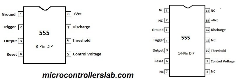
555 Timer Pinout Diagram
This picture shows the pinout diagram of the timer IC.

Furthermore, it is also available in the 14 Pin DIP package. This diagram represents pinout for 8-pin DIP and 14-pin DIP-packages. But, there is no difference between them except No connection of pins for 14 pins package.
Pin Configuration Details
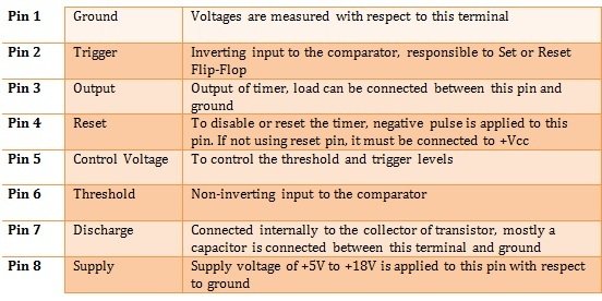
This IC is composed of a comparator, RS flipflop and a transistor. The description of pins is mentioned below:
- Pin1 and 8 are the supply pins and are connected to ground and positive voltage supply.
- Pin2 is the trigger input pin which is a negative pin of a comparator integrated inside the chip. The output depends on the amplitude of the value applied to this pin. When its value is less than 1/3 of supply voltage, it sets the internal flip flop which switches the output from low to high.
- Pin3 is an output pin of 555 timer IC.

- The reset pin is used to reset or disable the timer irrespective of the trigger input. In normal operation, it is connected to high voltage. When supplied with a low signal, it will reset the output.
- Pin 5 is a control input pin. As the name indicates, it is used to control trigger and threshold inputs. It is also used to control the width of the output pulse. It is connected to an external voltage to determine the width or modulate the output pulse. If you are not using a pin, connect a capacitor at this pin to avoid any noise issues.
- The threshold input is the positive pin of a comparator. Its amplitude is responsible for the set state of the flip-flop.
- Discharge pin is connected to low logic internally. It is used to discharge the capacitor when the transistor saturates.
FEATURES of 555 timer
It is used as
- Timers
- To provide time delays
- Pulse generation
- To toggle between high and low states
- Oscillator applications.
Other important features are:
- Wide range of power supply (5-18)V
- Sinking High current output (200mA of load current)
- Variable duty cycle
- Logic compatible trigger and reset inputs
- High-temperature stability
- The operating power supply range is from 5 Volts to 18 Volts.
- It can drive TTL as its output current is high.
- It has a capability of sourcing or sinking up to 200mA current
- Trigger and reset inputs are logic compatible.
- It has an adjustable duty cycle
- It has two outputs which are normally on and normally off.
- Turn off time is less than 2µ
555 timer Internal Circuit
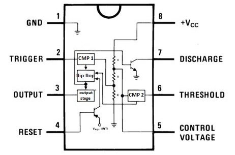
The internal circuit of this 555 timer consists of comparators, flipflops, transistors, resistors, and output stages.
555 Timer Working Principle
In this section, we will see the working of each internal component of the 555 timer IC.
Resistor
The three resistors used in it are of 5Kohm and they served as a voltage divider between Vcc and ground. All resistors are of the same value, so the voltage at the junction of the resistor is 2/3 Vcc and 1/3 Vcc which is used as a reference voltage for the comparators.
Comparator Circuit
It is a circuit that compares an input with a reference voltage (whether an input is a higher or lower voltage than a reference) and outputs a low or high signal. Many transistors are used for this comparator purpose. Trigger is the inverting input to the comparator 1. A threshold is a non-inverting input to the comparator 2. The comparator 1 connected to pin 2 compares the trigger input to a reference voltage of 1/3 of Vcc. The comparator 2 connected to pin 6 compares the threshold input to a reference voltage of 2/3 of Vcc.
FLIP FLOP Function
It is a circuit that can be in one of two states based on the state of inputs. The two comparators outputs are the inputs of a flip-flop. When the trigger comparator outputs a low signal (whatever the output of threshold comparator), the flip flop switches to high output. When trigger and threshold, both comparators are outputting a high signal, the flip flop switches output to low output. Time of high pulse output can be manually reset by pulsing the reset pin to low.
Transistors
Two transistors are also shown in the figure above. One transistor is N-P-N and its collector is connected to pin 7. This configuration is known as an open-drain or open collector. Usually, this pin is connected to a capacitor and is used to discharge the capacitor each time the output pin goes low. The second transistor is P-N-P which is connected to pin 4. The purpose of this transistor is to buffer the reset pin and so the 555 IC does not source current from this pin and causes it to sag in voltage.
Output Stage
It acts as a buffer between the 555 timer and the loads that may be attached to its output pin. This stage supplies current to the output pin.
Where to use 555 IC?
Due to its three operating modes, it can be used in a wide variety of applications for pulse generation, creating long time delays, voltage regulators, analog frequency meters and tachometers, control devices, multivibrators, oscillator circuits and many more.
555 Timer Different Modes of Operation
By wiring 555 timers with resistors and capacitors in different ways, It can operate in 3 modes:
- Monostable mode
- Astable mode
- Bistable mode
555 Timer MONOSTABLE MODE
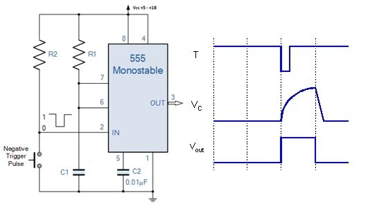
This mode is used for creating time delays. In this mode, the 555 timer outputs a high pulse. A monostable is a single stable state, i-e the off state. Whenever it is triggered by an input pulse, the monostable switches to its temporary state. It remains in that state for a period of time which is determined by an RC network. It then returns to its stable state.
- The trigger pin is set low (less than 1/3Vcc). Comparator connected to the trigger pin will have low output and sets the state of flip flop, changing output from low to high.
- The discharge transistor connected to pin 7 will get off. There will be no short circuit across the capacitor. A charge will build up across the capacitor until the voltage across the capacitor equals 2/3 of the supply voltage (Pin 6 voltage= 2/3 Vcc).
- Now at this point, the output of the comparator goes “HIGH. This will reset the flip-flop back to its original state (low).
- Now transistor gets ON and discharges the capacitor to ground through pin 7. This causes the output to change its state back to the original stable (low).
- The output remains low until the trigger pin is pulsed low again.
- The amount of time that the output voltage remains “HIGH” or at a logic “1” level is given by the following time constant equation.
555 IC ASTABLE MODE

This mode outputs an oscillating pulse signal. The output switches between high and low states at a tunable frequency and pulse width. Frequency depends on the values of the two resistors (R1 and R2) and capacitor C1. Trigger pin is connected to the threshold pin which causes the output to continuously toggle between the high and low states.
Frequency of Output = 1/[0.7*(R1+2*R2)*C1]
duty cycle = (R1+ R2) / (R1 + 2*R2)
- Initially, there is no charge on the capacitor C1, so the voltage across the capacitor is zero. Since capacitor C1, Threshold pin and Trigger pin are connected at the same, so these both will also be at zero volts. This drives the output high.
- Vcc is applied, the current flowing through resistors start to accumulate charge on the capacitor C1. This causes the voltage across capacitor C to increase.
- When the voltage across the capacitor C1 equals 2/3Vcc, it makes the threshold pin high, this flips the comparator attached to the threshold pin. This drives the output low and enables the discharge pin.
- When the discharge is pin enabled, the capacitor will discharge through R2.
- Once the voltage across the capacitor C1 equals 1/3Vcc, it makes the the trigger pin low. This flips the comparator attached to the trigger pin and drives the output high. By repeating above steps, the output switches between the high and low states to produce a continuous pulse wave.
555 Timer BISTABLE MODE
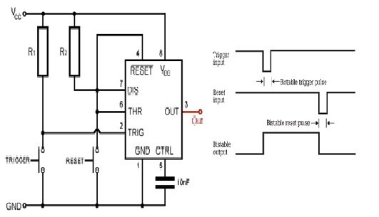
This mode causes the 555 timers to toggle its output between high and low states depending on the state of two inputs. The circuit is stable in both states. It remains in the same state (either HIGH or LOW) until an external trigger is applied.
- In this mode, there is no RC network like the other two modes of 555, hence there are no equations.
- This circuit is actually a flip-flop.
- The two inputs are the trigger (pin2) and reset pins (Pin 4).
- By default, both are kept high by pull up resistors in bistable mode.
- When the trigger pin is pulsed low, (less than 1/3(Vcc)), it gives a high output. The output will remain high even if the trigger pin is set high again.
- When the reset pin is pulsed low, the output goes low. The output will remain in this state even if the reset pin goes high again.
555 timer Proteus Simulations
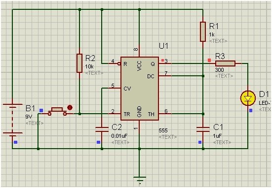
Example Circuit 1
Here, we are using 555 timers in monostable mode. When the trigger pin is set low, it gives high output and then output goes low.
As the name indicates, it consists of one stable and one unstable state. It is used to produce a predefined length of a pulse by applying a triggering input. The output remains in a low state before applying a trigger input. You can connect a supply using push-button at trigger input pin. When the push button is pressed, the output will become high and returns back to its original state after a certain time period which can be determined by selecting appropriate values of the resistor and a capacitor. The following equation is used to set the values of R and C to obtain the desired time period.
Example Circuit 2
Here, we are using 555 timers in astable mode. When the trigger pin is set low, it gives high and low output pulses.

In this mode, the output is not stable. It produces a continuous stream of a square wave having a specific frequency at output whose value keeps on changing between high and low values. In this mode, a control pin is not used that is why it is connected to ground through a capacitor which is used to avoid electrical noise. The reset pin is connected to the positive supply. Pin 2 and pin 6 are connected together. It is used to switch ON and OFF the motors and that is how you can control the speed of motors. A constant square wave is obtained at the output which is also used in relaxation oscillators.
Example Circuit 3
In this mode, both the output states are stable. Pins 2 and 4 are connected to push buttons. Pin 6 is grounded. This mode is used to perform only two operations On or off. Pin 2 is active low when its value is greater than 1/3 of supply voltage, it makes the output high.
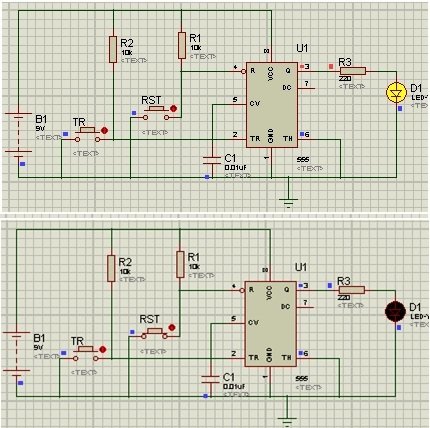
Here, we are using a 555 timers in Bistable mode. When the trigger pin is set low, it gives high output and will remain in that state until the reset button is pressed. When reset is pressed it gives low output. Again we can make the output high by pressing the trigger button.
555 Timer Applications
Some common applications of this IC are:
- Pulse generation
- Pulse width and pulse position modulation
- Sequential Timing circuits for precise timing or pulse generation
- Oscillators and as a flip flop
- Analog frequency meters.
2D diagram
It has 8-lead PDIP, SOIC, and VSSOP packages available. The dimensions and 2d diagram of its PDIP package is given below.

Datasheet
Related Tutorials:
Thanks so much