Recommended Components
The following parts are used in this article, along with a generic electronics kit that is handy for building and testing the circuit.
| Component | How it’s used | Buy on Amazon |
|---|---|---|
| IR2112 MOSFET/IGBT gate driver | The IR2112 high/low-side MOSFET & IGBT gate driver this article covers. | Check Price |
| Electronic component assortment kit (1390 pcs) | A handy assortment of resistors, capacitors, LEDs, diodes and transistors for building circuits. | Check Price |
| Digital multimeter (AstroAI) | Measures voltage, current, resistance and checks continuity while you build and debug. | Check Price |
| Breadboard | Solderless base for prototyping the circuit. | Check Price |
| Jumper Wires | Make the connections on the breadboard. | Check Price |
As an Amazon Associate we earn from qualifying purchases. Prices and availability are accurate as of the date/time indicated and are subject to change.
IR2112 Pinout Diagram
IR2112 pinout diagram shows that it consists of 14 pins. LO and HO are output pins for low and high side respectively. LIN and HIN are input pins for drive signals such as PWM, SPWM. The rest of the descriptions of the pins are given in pin configuration section.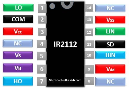
Pin Configuration Details
The driver IC has 14 pins whose functionalities are mentioned in the table given below:| Pin Number | Pin Name | Description |
|---|---|---|
| 1 | LO | Gate drive output of Low voltage side |
| 2 | COM | Return path for low side driver |
| 3 | Voltage supply for low voltage driver and its value should be between the range of 10V to 20V. | |
| 4, 8, 14 | NC | No connection for these pins and no use |
| 5 | Vs | Floating point return path for low side |
| 6 | Floating point for high side drive | |
| 7 | HO | Gate drive output for high driver side |
| 9 | Voltage supply and its value should be in a range of +3V to +20V with reference to ground or Vss. For normal operation, we use = +5V. | |
| 10 | HIN | In phase input logic signal for gate output of high side driver |
| 11 | SD | Input signal for shut down |
| 12 | LIN | In phase input logic signal for gate output of low side driver |
| 13 | Vss | Ground of the circuit |
IR2112 MOSFET/ IGBT driver Features
- High and Low Side Driver IC with source current 0.25 A and sink current 0.5 A
- It can tolerate negative transient voltage
- The range of separate voltage supply is from 3.3V to 20V and supply range of gate driver is from 10 to 20 V
- It has a feature of floating channel which can perform bootstrap operation
- Inputs and outputs are in phase
- Matched propagation delay and undervoltage lockout for both channels
- Threshold voltage is +600 V
- Cycle by cycle edge-triggered shutdown logic
Equivalent options
- IR2110
- IR2118
- IR2101
- IR2102
- IR2104
- IR2106
- IR2184
Where to use IR2112?
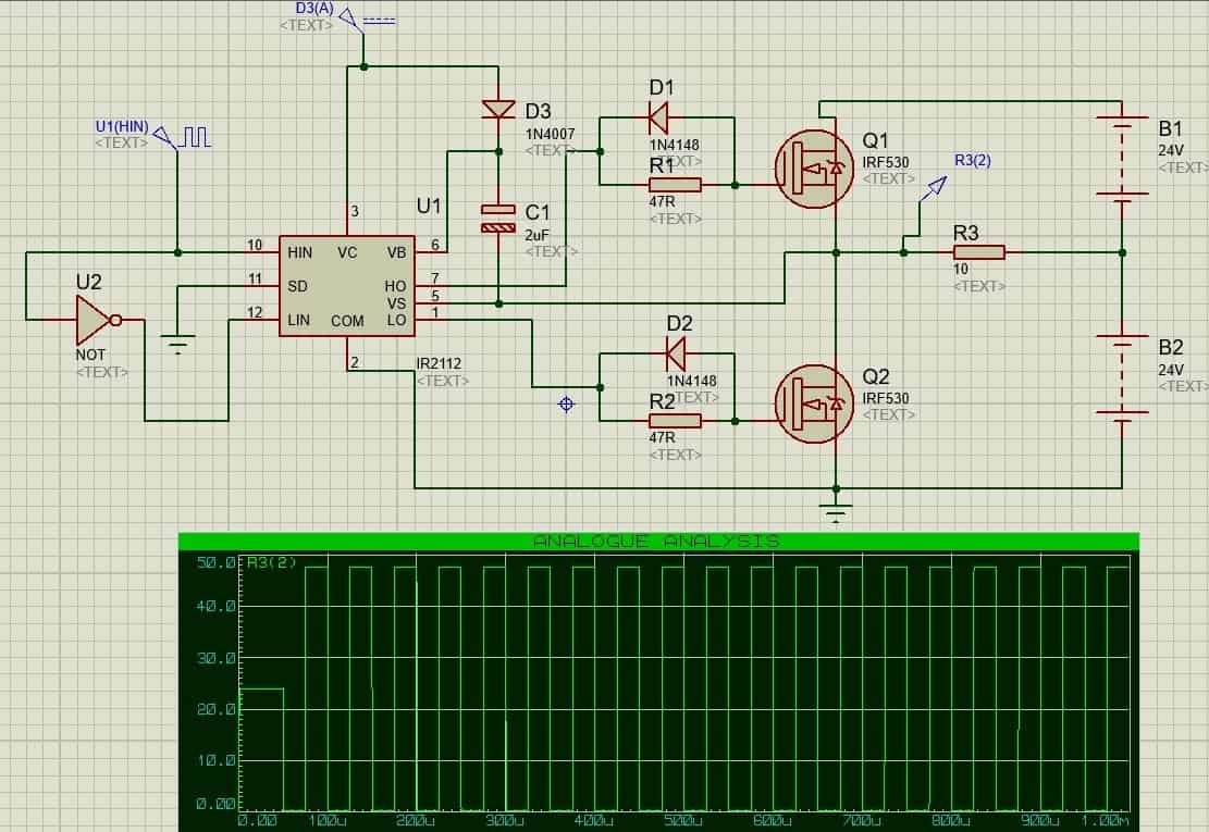
This IC can be used as both Mosfet driver and IGBT driver. These IC’s are commonly used in half-bridge circuits for switching Mosfets. You can use this IC in high-frequency applications due to its matched propagation delays. It is used in high voltage applications for switching discrete power Mosfets ON and OFF using low voltage input.How to use IR2112 MOSFET/IGBT Driver?
The connection diagram of this IC 12R2112 are shown in the figure below. HIN and LIN are the input signals for high and low driver side. They connect to some microcontroller or a voltage supply through a switch and is provided with an input signal of range 4 to 5V. It has a shutdown pin which is provided to protect the circuit in case of over voltages or current by connecting this pin to +5V. It will shut down the circuit.Bootstrap Capacitor
You can see a capacitor between and Vs from the figure below. This is a bootstrap capacitor and its function is to fully operate the high driver side of Mosfet. One end of the bootstrap capacitor is connected to the diode. The doide will charge the capacitor and prevent discharging when is High. For proper switching of the mosfet gate, this capacitor should be charged up between 10 to 20V. After connecting all the input pins, switch ON the power supply.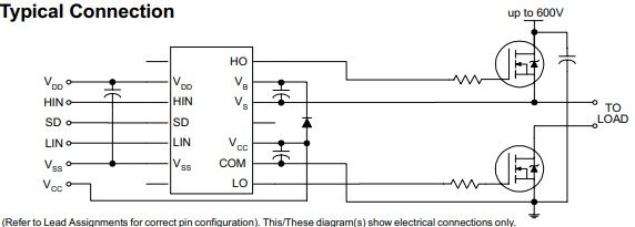 If you want to drive high side MOSFET, connect HIN to High signal and HO pin will produce HIGH output. To turn-off the high side, apply low signal on HIN pin. Same is the case of LIN pin. When Vs is HIGH, the output at HO will be equal to Vb level, with respect to Vs, When Vs is LOW, the value on HO will be equal to Vs with reference to Vs which means 0 logic.
Example circuit as a half-bridge
IR2112 Applications
This IC has numerous applications especially switching circuits. Some of its applications include:- Designing H-bridge, half-bridge, and full-bridge circuits
- Switched-mode power supplies
- Inverters, traction motor control, and induction heating.
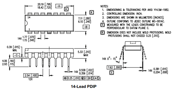
2D Diagram
Like!! Thank you for publishing this awesome article.